PCB silkscreen
By:PCBBUY 05/26/2021 17:45

During the manufacturing process of PCB product, silkscreen is marking ink used to identify components during later assembly and troubleshooting processes. This can be placed on one or two sides (in yellow or white), depending on the board design and application.
The silkscreen layer is the top layer of the PCB and serves as a reference indicator for placing components on the PCB. Screen printing is used to specify useful information on the PCB board, which can help users during the assembly. It is used to mark component values, part numbers, test points, polarity, etc.
The problems related to the material of silkscreen are rarely occurred, except maybe some discoloration after high PCB reflow temperatures for RoHS compliant soldering. Silkscreen problems are always caused by the design of the PCB.
What Is the Importance of PCB Silkscreen?
In the past few years, the primary method of silkscreen referred to using a stencil to directly apply ink to the board surface. Nowadays, there are the two most common silkscreen PCB printing techniques, such as liquid photo imaging (LPI) and direct legend printing (DLP).
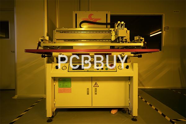
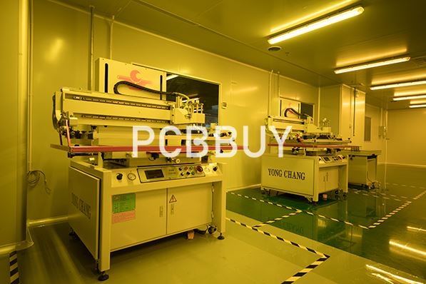
Manual Screen-printing
Manual screen-printing is done when the line widths are greater than 7 mil (0.007”) and the registration tolerance is 5 mil. For this method you require a stencil of the text and traces made of nylon. The ink is pushed through the stencil onto the laminate. Next the board is baked in a curing oven for the ink to cure.
Liquid photo imaging (LPI):
This method is used when the line widths are greater than 4 mil. Liquid Photo Imaging is quite similar to the process used for the application of solder mask. In this a liquid photo-imageable epoxy is coated on to the laminate and then exposed with UV light. After this the board is developed and cured. It is much more accurate than manual screening.
Direct legend printing (DLP):
DLP is the most accurate of all these processes but is more expensive. In this process an inkjet projector is used with acrylic ink that is applied onto the raw PCB directly from the CAD data. The ink is cured with UV light as it is printed. It should be noted though that the acrylic ink does not cure on boards with silver finishes.
The application of PCB silkscreen is done during PCB fabrication, but it’s used for the PCB assembly process steps, which is mainly in referring to placing or mounting components. There are some silkscreen markings used to accurately place components as follows:
Reference indicators - these identify the component types from the BOM.
Pin 1 indicator - this indicates which pins connect to what pads of the footprint.
Component outline – this, in conjunction with the landing pattern, indicates where the component should be placed.
Polarity indicators – these provide the orientation of polarized components.
For components with small numbers of pads or simple shapes, it may be acceptable for general placement to have the absence of the component outline. However, there still exists the possibility of asymmetrical placement, which may lead to problems during soldering, for example tombstoning. The absence of reference, pin 1 and polarity indicators may lead to incorrect component orientation or placement, which could have a negative effect on device functionality.
What Are Tips for PCB Silkscreen?
As discussed earlier, using a silkscreen PCB layout is an important aspect of board design and not including it can cause serious problems for PCB assembly and testing. The silkscreen is also used for labeling, which may include manufacturer information, testing certifications, model or serial numbers. In order to be effective and useful, the silkscreen must have clearly readable text, provide sufficient image resolution and, most importantly, be accurate. Here are a few tips to help you ensure that your silkscreen PCB layout can be used for its important roles in PCB assembly, testing and identification:

Tip 1: Only use fonts approved by your CM as some fonts, although easily created in software, are difficult to generate during board manufacture.
Tip 2: Use white or black instead of other colors to provide the best contrast with your board’s solder mask color.
Tip 3: Make sure to follow your CM’s clearance and dimension guidelines. This will ensure that your silkscreen items do not get covered by components and are easily visible.
Industry Category


