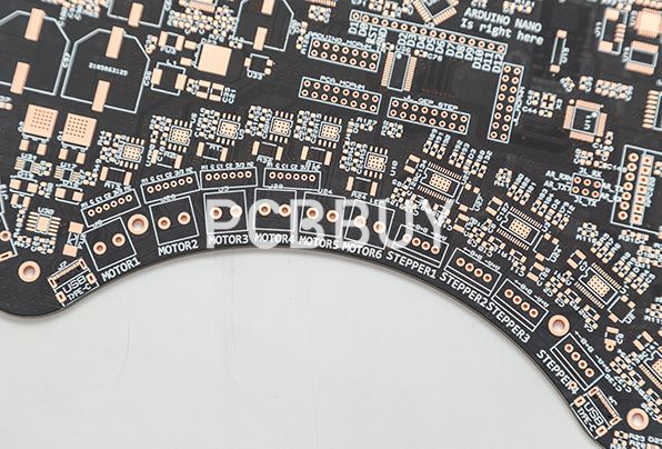
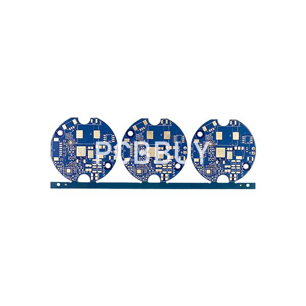
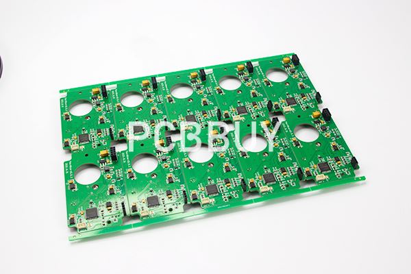
PCB solder mask
By:PCBBUY 05/14/2021 18:00

Solder mask is a thin layer of polymer that is put on a circuit board to protect the copper from oxidation and shorts during operation. It also protects the PCB from environmental influences such as dust and several other contaminants that may lead to shorts in the long run.
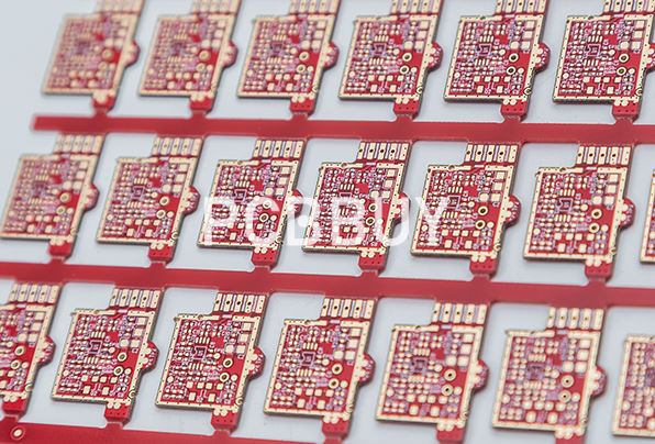
Solder mask or solder stop mask or solder resist is a thin lacquer-like layer of polymer that is usually applied to the copper traces of a printed circuit board (PCB) for protection against oxidation and to prevent solder bridges from forming between closely spaced solder pads. A solder bridge is an unintended electrical connection between two conductors by means of a small blob of solder.
PCBs use solder masks to prevent this from happening. Solder mask is not always used for hand soldered assemblies, but is essential for mass-produced boards that are soldered automatically using reflow or solder bath techniques. Once applied, openings must be made in the solder mask wherever components are soldered, which is accomplished using photolithography.Solder mask is traditionally green but is now available in many colors.
What are main types of PCB solder mask?
Top and bottom side masks
These are typically used by engineers to identify openings in the green solder mask, already applied on the PCB. This particular layer of solder mask is added through epoxy or film methods. Next, the component pins are soldered to the board utilizing the openings that have been registered using the masks.
The traces on the top-side of the board are called top traces and the corresponding solder mask used is called a top-side mask. Identical to the top-side mask, the bottom mask is used for the bottom side of the board.
Epoxy liquid solder masks
The most cost-effective option among solder masks is epoxy. It is a polymer that is silkscreened on the PCB. Silkscreening refers to a printing technique that uses a woven mesh to support ink-blocking patterns. The mesh enables the open areas to be identified for the process of ink transfer. This step is then followed by thermal curing.
Liquid photoimageable (LPI) solder masks
LPI solder masks are actually a mix of two distinct liquids. These liquids are kept separately and mixed right before the application of the mask layer to enable longer shelf life. LPI is also one of the more cost-effective options among various other types.
LPI is employed for curtain coat, screen printing, and spray applications. This mask is a blend of various polymers and solvents. A thin coating can be formed using this mask that can stick to the target area surface. After using this mask, the PCB will generally not require any final surface finish that is currently available.
Unlike conventional epoxy inks, LPI is sensitive to UV light. The panel is required to be covered with the mask and after a short ‘tack cure cycle’, the PCB is exposed to UV light using a UV laser or photolithography process.
Before mask application, the panels are subjected to cleaning and are checked for any sign of oxidation. This is done using a chemical solution, aluminum oxide solution, or using suspended pumice to scrub the panels.
One of the most popular techniques used to expose the panel surface to UV light is through the use of film tools and contact printers. The top and bottom sheets of the film are printed using emulsion to block areas that need to be soldered. Production panels and film are then fixed in position, making use of tooling on the printer and exposed to a UV light source simultaneously.
One method utilizes direct imaging that makes use of a laser. This technique does not need tooling or film as the laser is controlled through the use of fiducial markers placed on the copper template of the panel. LPI masks are available in various colors such as green, black, red, yellow, white, and blue.
Dry film photoimageable solder masks
The use of dry film photoimageable solder masks requires vacuum lamination. This dry film is subjected to exposure and then developed. Post-development, openings are identified to generate a pattern, after which the components are soldered to the copper pads. High-density wiring boards benefit most from dry film solder masks as it does not flood the through-holes.
How the solder masks influence PCB?
Now that we have delved into the solder mask process, let’s examine how this process affects your PCB. As previously stated, the solder mask impacts PCB assembly and board quality. The most notable impacts of solder mask are listed below:
Prevention of solder bridges
Provides a solder dam between solder joints and other conductive areas of the board where Solder bridges may form, potentially leading to short circuits or board damage.
Reduction of solder paste consumption
Allow less solder paste to be used during solder process.
Additional insulation of the components from PCB
Serve as an insulator between board components.
Protection of the PCB
Guard against contaminants that may be introduced from handling the board.
Prevents oxidation that may shorten the operational lifetime of the device.
Increasing the breakdown voltage
May increase the breakdown voltage of the board’s dielectric material.
Prevention of metal whiskers
Help prevent the growth of tin whiskers mostly associated with lead-free solder or tin-plating for electronic components.
Industry Category


