PCB tenting vias
By:PCBBUY 07/07/2021 16:56

Do you know the difference between different tenting and plugging techniques? In this passage we will lead you to learn the professional knowledge about tenting vias. Please come and check the content we prepare for you.
What is the definition of tenting vias?
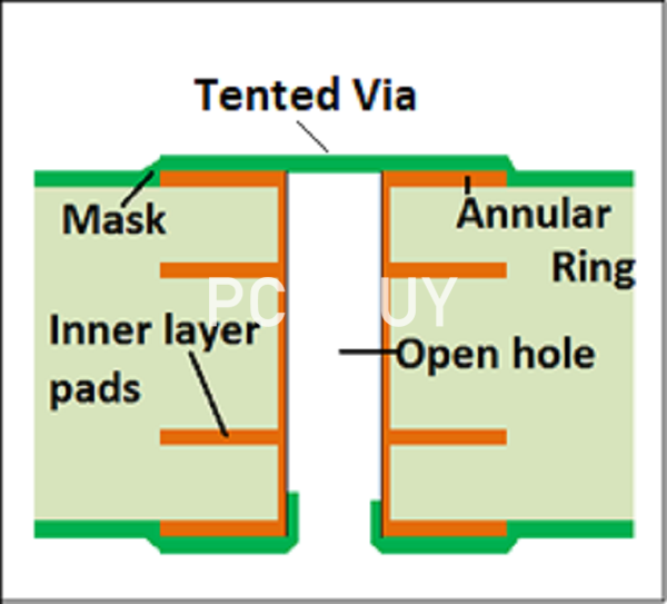
Vias can be very negligible in size, but they are crucial parts of a printed circuit board (PCB). Vias are used to interconnect the copper traces present on different layers of a multi-layered PCB. You will never find any component lead passing through the hole of a via. There are different types of vias, and drilling holes on the PCB make all of them.
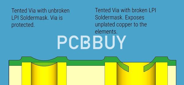
A via may be tented or left exposed — a tenting of a via means that solder mask has been used to cover the via over the hole in the shape of a tent or a skin. Earlier, manufacturers had to face difficulty in tenting the vias as they used liquid photo-imageable (LPI) solder mask. But with the introduction of the dry film solder mask, the process has become much more comfortable.
Tenting a PCB brings down the number of exposed conductive pads and reduces the chances of shorts arising from solder bridging. It also protects the vias from corrosion and external elements. When dealing with SMT pads, tenting is useful to lessen past migration from the SMD elements when the vias are designed at the end of places.
Tenting is also ideal for vias located close to SMT pads, reducing the chances of short that occur during reflow. Sometimes, the tented via is again given a coat of solder mask.
Why is PCB tending via important?
Tenting vias of a printed circuit board is a common practice to protect printed circuit boards. It is often preferred over mask plugging or epoxy filling because of cost. The most cost-effective form of via tenting is LPI, or liquid photo imageable solder mask tenting. If you’re very concerned about the tenting coming loose and exposing the annular ring, you may choose to use a somewhat more expensive resin filling.

The main goal of via tenting is to leave fewer exposed conductive pads on the surface of your printed circuit board. This should, in turn, mean fewer shorts brought about during solder bridging during assembly. Another benefit is a reduction of paste migration from SMT pads, which can occur when vias are drilled on standard BGA “dog-bone” patterns or when the vias are on the edges of SMT pads. Tenting will also help ensure that the via is less likely to be damaged by exposure to the elements.
Tenting is usually more effective with smaller vias (diameter of 12 mil or less), so if you have larger vias that you need to protect, you may want to consider some kind of fill to close the via instead. Filling your vias will not usually significantly affect conductivity as electrical travel through the copper plating is unimpeded.
What are the benefits of tending via?
The foremost advantage that tenting vias offers is the protection offered by the solder mask. The tenting creates a barrier that ensures there aren’t any damages to the PCB layers. This is akin to how the solder mask prevents corrosion in the copper traces.
Another advantage of the tenting method is also that the numbers of exposed conductive components are minimized. The exposure of these components can result in corrosion. Tenting also helps in significantly bringing down the possibility of a short on account of the solder bridging. With tenting, you can also rest assured that the paste migration from SMT pads is significantly reduced. The fact that tenting is a cost-effective method of protecting the vias is an added perk!
Limitations
A major limitation of the tenting process is that with a liquid solder mask, there is always the possibility of breaking of LPI and creating small holes in the tent. In turn, these holes can trap moisture and corrosion can be the natural outcome.
To overcome this limitation, it is important that the vias are left exposed in the prototype stage. That way, any issues can be identified and the traces can be fixed. With covered vias the opportunity to discover these issues is significantly limited.
How to make the decision to tent via?
Two major aspects go in to decide whether or not you should tent via. The first, of course is the PCB design and the second is the size of via.
As a thumb rule, tenting works well with vias of smaller diameters of 12 mil or less. Any via that is above 12 mil in diameter does not lend itself to tenting. If you need to take care of large vias closing it with some kind of fill is a far better alternative.
Tenting is also preferred on account of its lower cost as opposed to mask plugging or epoxy filling. In fact tenting via with a liquid photo-imageable solder mask turns out to be the most cost-effective. However where there are concerns about tenting being loose, epoxy filling is an alternative, even though it comes at a higher cost.
Industry Category


