Text point in PCB
By:PCBBUY 05/22/2021 17:15

The PCB testing will determine how well they have been manufactured. In order for this testing to happen, the board must be prepared with specific elements that a test probe can access. These elements are called test points and their inclusion on PCB designs is very important. Let’s take a few minutes here to talk about the PCB test point and why it is so important to the success of the completed circuit board.
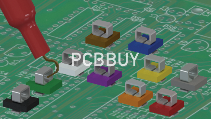
A PCB test point is a small wire loop used for test probes on a PCB that contains surface-mount parts. During production, they enable the user to inject test signals or monitor the board’s circuitry. Test points come in a variety of materials, sizes and colors.
With a test point, you can create an access area for your test probe. Many of these probes have J-hooks designed for older PCB styles that included leads. A PCB test point provides a place for the J-hook or has a sharp pointed end that touches a conductor on the board. Most surface-mount test points feature a phosphor bronze alloy, but they can also have more affordable silver plate coatings.
What Are the Different Types of PCB Test Points?
There are two main types of test points used on a printed circuit board. The first is an easily accessible point for a technician to access with hand-held testing equipment. To help with this, these points often have a post soldered into them for clipping on a test lead. These test points will be marked with a reference designator and usually the name of the net in silkscreen for easy reference, such as “GND.”
The other type of test point is used primarily for automated test equipment. The automated test points on a circuit board are thru-hole pins, vias, or small landing pads of metal that are designed to accommodate the probes of automated test systems. There are three main test systems that will use these test points on the board:
Bare board test: This is a test that is run after the circuit board has been fabricated to make sure that all of the nets in the board have electrical connectivity.
In-circuit test: ICT is run after the board has been assembled. The board is positioned on the ICT fixture which is filled with probes for each individual net. These fixtures usually test the bottom of the board, but they can also test the top or both sides together if needed.
Flying probe: Like ICT, this test is run after assembly on each net of the board by accessing the test points. Where it differs, however, is that the flying probe equipment uses two to six probes that move around to each test point instead of using stationary probes in a fixture like ICT does.
Those are the different test points that will be included in a PCB design and what they are used for. Next, we will see why this testing is so important for circuit board manufacturing.

Why Test Points Are Important for PCB Manufacturing?
Automated testing is essential for verifying the manufacturing of printed circuit boards. While a bare board test checks that the fabricated PCB board has good connectivity, ICT and flying probe tests will verify the board assembly and solder connections. Here is how ICT and flying probe testing accomplish that:
In-Circuit Test (ICT)
ICT is a system that uses a test fixture that is prepared exclusively for a specific circuit board design as well as accompanying software that will be run on the test system. The fixture and software are created using the test point locations and other design data generated by the CAD database, and a probe will be used for each net on the design. While the main purpose of ICT is to verify the assembly of the board by testing each net for a good connection to its associated part pin, it can also be used to test the functionality of the board.
ICT test fixtures and software are expensive and time-consuming to develop. The test fixtures are complex with thousands of probes in them and changes to a fixture for board revisions can also be very expensive. Once developed, though, the in-circuit test will test large amounts of circuit boards very quickly. For mass production, the benefits of speed and functional testing quickly offset the development time and costs of ICT.

Flying Probe Testing
This system is also designed to verify the integrity of an assembled circuit board, but it does this very differently than ICT. Instead of a test fixture, there are only two to six probes that fly around accessing each test point on the board. Without the need to build an expensive test fixture, the flying probe system can be set up very quickly and inexpensively. Also, any changes to the board that require changes to the test system can be easily reprogrammed.
The disadvantage of the flying probe is that it is very slow. Where ICT can test all of the points on the board almost instantaneously, the flying probe system has to maneuver its probes around to each individual test point. On a large board, this can take a very long time, and the ability to do functional testing is eliminated. However, for prototypes or low volume production runs, using the flying probe for testing can be very advantageous.
Now that we’ve seen what test points are and how they are used, we’ll next look at how PCB CAD tools include them in the design.
Industry Category


