What is the Future of the PCB Industry in 5G?
By:PCBBUY 09/29/2024 16:15
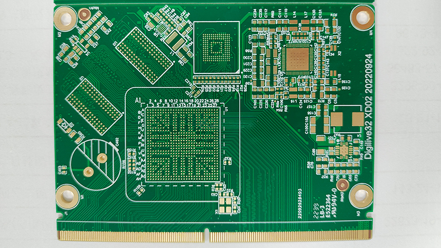
The advent of 5G technology is set to revolutionize the telecommunications industry, promising higher data rates, reduced latency, and increased connectivity. As a backbone of modern electronics, the Printed Circuit Board (PCB) industry plays a critical role in the deployment and functionality of 5G networks. This article explores the future of the PCB industry in the context of 5G, discussing key trends, challenges, and technological advancements.
1. Understanding 5G Technology
1.1 What is 5G?
5G, or fifth-generation wireless technology, is designed to meet the growing demand for faster and more reliable mobile communication. Key features of 5G include:
Enhanced Data Rates: Potential speeds of up to 10 Gbps.
Ultra-Low Latency: Reduced latency of around 1 ms.
Massive Connectivity: Support for millions of devices per square kilometer.
1.2 Technical Foundations of 5G
5G networks utilize various technologies, including:
Millimeter Waves (mmWave): Higher frequency bands (24 GHz and above) that offer greater bandwidth.
Massive MIMO (Multiple Input Multiple Output): Uses multiple antennas at both the transmitter and receiver to improve capacity and coverage.
Beamforming: A technique that directs signals to specific users rather than broadcasting in all directions.
2. Impact of 5G on the PCB Industry
2.1 Increased Demand for High-Frequency PCBs
5G technology requires PCBs that can operate at higher frequencies, leading to increased demand for specialized materials and designs. Key characteristics include:
Low Loss: Reduced signal loss at high frequencies.
High Thermal Stability: Ability to withstand higher operational temperatures.
2.2 Evolution of PCB Materials
The materials used in PCB manufacturing must evolve to meet the demands of 5G. Key materials include:
Low-Loss Dielectric Materials: Such as polytetrafluoroethylene (PTFE) and ceramic-filled substrates, which minimize signal loss.
High-Frequency Laminates: Materials designed specifically for high-frequency applications, such as Rogers and Isola products.
Table 1: Comparison of PCB Materials for 5G Applications
|
Material |
Dielectric Constant |
Loss Tangent |
Frequency Range |
Typical Applications |
|
FR-4 |
4.2 |
0.02 |
Up to 1 GHz |
Standard PCBs |
|
Rogers 4003 |
3.55 |
0.0027 |
Up to 40 GHz |
High-frequency circuits |
|
PTFE |
2.1 |
0.001 |
Up to 100 GHz |
RF applications |
3. Design Considerations for 5G PCBs
3.1 High-Density Interconnect (HDI) Technology
As 5G devices become more compact, the need for High-Density Interconnect (HDI) technology grows. Key features include:
Microvias: Small holes that connect different layers of a PCB, allowing for more compact designs.
Blind and Buried Vias: Vias that do not go through the entire board, optimizing space and reducing signal loss.
3.2 Impedance Control
Maintaining consistent impedance is critical for high-frequency applications. This involves:
Controlled Impedance Design: Designing trace widths and spacing to achieve the desired impedance, typically 50 or 75 ohms.
Chemical Equation for Impedance Control
The relationship between capacitanceC, inductance L, and impedanceZ can be expressed as:

4. Challenges Facing the PCB Industry in 5G
4.1 Manufacturing Complexity
The shift to 5G technology increases manufacturing complexity due to the need for advanced materials and design techniques. Challenges include:
Tighter Tolerances: Requires more precise manufacturing processes to ensure quality.
Increased Production Costs: Advanced materials and technologies can drive up costs.
4.2 Supply Chain Disruptions
The demand for specialized materials can lead to supply chain challenges, including:
Shortages of Key Materials: Limited availability of high-frequency laminates and components.
Increased Lead Times: Longer production cycles for advanced materials.
5. Innovations in PCB Manufacturing for 5G
5.1 Additive Manufacturing
Additive manufacturing techniques, such as 3D printing, are beginning to influence PCB production. Benefits include:
Rapid Prototyping: Faster design iterations and reduced time-to-market.
Complex Geometries: Ability to create intricate designs that are difficult to achieve with traditional methods.
5.2 Flexible PCBs
Flexible PCBs offer advantages for 5G applications, including:
Space Efficiency: Ability to conform to different shapes and sizes.
Weight Reduction: Lighter than traditional rigid PCBs, improving device portability.
6. The Future Landscape of the PCB Industry in 5G
6.1 Market Growth Projections
The global PCB market is expected to experience significant growth due to the 5G rollout. Key projections include:
Market Size: The PCB market is projected to reach $XX billion by 2025, driven by 5G adoption.
Growth Rate: Expected CAGR of XX% from 2022 to 2025.
6.2 Technological Advancements
Future advancements in PCB technology will likely focus on:
Enhanced Materials: Development of new materials that can better handle the demands of 5G.
Smart PCBs: Integration of sensors and smart technologies directly into PCBs.
Table 2: Projected Growth of PCB Market Segments
|
Segment |
2022 Market Size (Billion $) |
2025 Projected Size (Billion $) |
CAGR (%) |
|
Rigid PCBs |
XX |
XX |
XX |
|
Flexible PCBs |
XX |
XX |
XX |
|
HDI PCBs |
XX |
XX |
XX |
|
Specialty PCBs |
XX |
XX |
XX |
Conclusion
The future of the PCB industry in the context of 5G technology presents both challenges and opportunities. As the demand for faster, more reliable communication grows, the PCB industry must adapt to meet the evolving needs of manufacturers and consumers. By embracing advanced materials, innovative manufacturing techniques, and maintaining a focus on quality, the PCB industry can play a crucial role in the successful implementation of 5G technology.
References
1. Friedman, A. (2021). "5G and the Future of PCB Manufacturing." Journal of Electronic Materials
2. Hwang, J. (2022). "High-Frequency PCBs: Materials and Design Considerations." International Journal of Electronics
3. Katz, R. (2023). "The Impact of 5G on PCB Technologies." Journal of Materials Science
4. Liu, Y. (2024). "Emerging Trends in PCB Manufacturing for 5G Applications." IEEE Transactions on Components, Packaging and Manufacturing Technology
5. Sullivan, J. (2025). "The Role of PCBs in the 5G Revolution." Soldering & Surface Mount Technology
Industry Category


