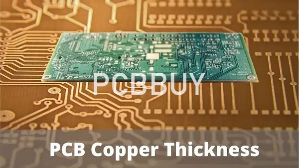
What is the Standard Thickness of a Copper Layer on a PCB?
By:PCBBUY 10/10/2021 10:12

The fabrication of the copper traces of your board, whether on the surface or for internal layers, is done by etching, one of the major PCB manufacturing steps. Layer fabrication begins with a laminate sheet that is completely covered by copper. Etching is the process of removing excess copper from traces and other areas, such as component pads and annular rings for vias, using an ammonia-based solution.
If you are looking for the copper thickness of PCB, please check and read this passage for more professional knowledge in the content below.
Why copper is used in PCB?
There are two similar terms used in PCB design; copper balancing and copper thieving. Although they are often used interchangeably, there are some important distinctions between the two:
Copper balancing
This is the process of adding non-conductive patterns of copper to a circuit board in order to alleviate the possible bending of the board during manufacturing. PCB layer stackups that are not configured symmetrically, or individual layers with dense copper on one side versus the other, can all cause the board to warp during fabrication. Uneven copper in the board structure can also twist during the assembly process due to the excessive amount of heat used for soldering. To counter this, the PCB CAD design system will add area fills, or pours, to sparse areas of the board to copper balance the design.
Copper thieving
This is also the addition of non-conductive patterns of copper to the circuit board, but in this case, it is to even out or “thieve” some of the electrical current used for plating the board. On areas of the board where there are isolated or “lonely” traces, the current applied to the board for plating can become more concentrated on those features. This scenario may result in an under-etching of the trace giving it a “mushroom” profile instead of the clean squared edges that were expected. You can see an example of this in the image below, where the cross-section of the trace on the left depicts serious undercutting, while the trace on the right is more squared off as desired.
How to choose correct material for PCB copper?
Copper Foil
Copper foil is a cathodic electrolytic material deposited on a thin, continuous layer of metal foil on the base of the circuit board. It is easily bonded to an insulating layer, accepting a printed protective layer, and corroded to form a circuit pattern.
Prepreg
A prepreg (from pre-impregnated) is fibreglass impregnated with resin. The resin is pre-dried, but not hardened, so that when it is heated, it flows, sticks, and is completely immersed. Prepregs are thus fibreglass strengthened by an adhesive layer (similar to FR4 material). The name of each prepregs derives from the type of fibreglass used.

What is the standard PCB copper thickness?
The most common unit of measure for the copper thickness on a printed circuit board is ounces (oz). But most of people have no idea about how thick is it. It's the finished thickness when 1 oz copper is pressed flat and spread evenly over a one square foot area, which equals 1.37 mils. Of course not everyone thinks in mils so you can convert into your preferred unit of measure with our unit conversion tool.
Most printed circuit boards are constructed with 1 oz copper thickness. In PCB manufacturing, if customers do not offer specific specs, we will assume 1 oz when quoting and building the design. If customers have decided that the design requires more current than 1 oz can carry, it would better to consider increasing the copper thickness or increasing the width of your traces. Of course the thicker the copper the higher the cost, but there are certainly times if it is necessary. The cost increase is not only due to the raw material costs but processing thicker copper weights takes more time and is a little trickier to do.
How to process PCB copper thickness?
The manufacturing of the copper traces of your board, whether on the surface or for internal layers, is done by etching, one of the major PCB manufacturing steps. Layer fabrication begins with a laminate sheet that is completely covered by copper. Etching is the process of removing excess copper from traces and other areas, such as component pads and annular rings for vias, using an ammonia-based solution.

Typically, these sheets begin with preset copper thicknesses. This thickness can be etched down, decreased, or plated up, increased, to the desired specification. Due to the manufacturing process for the sheets, the surface has a degree of roughness that helps with bonding to the dielectric material. However, this can have an increasingly adverse effect on signal integrity at higher frequencies. At frequencies above 100MHz, the skin effect, where current flow is typically near the internal surface of the trace as opposed to through the conductor center, occurs, causing the effective resistance of the trace to increase and oppose current flow.
Industry Category


