PCB tombstone effect
By:PCBBUY 07/20/2021 17:42

In the reflow soldering of SMT, the components will desoldering because of warp. This is Manhattan effect. We call it “tombstone”. Manhattan effect usually appears in the reflow soldering process of CHIP components (such as capacitor and resistor). The smaller the component, the more likely it is to occur. And the reason is: When the solder paste on the solder pads at both ends of the component is melted in reflux, the surface tension of the two soldered ends of the component is unbalanced.
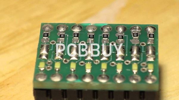
Before welding, the two ends of the chip Multi-layer Ceramic Capacitors (MLCC) are temporarily positioned with solder paste and board pads. When the welding is successfully completed, they become part of the assembled circuit board. Once the two ends are unevenly wetted when melting tin, the uneven surface tension generated on the two ends will cause one of the ends to slide off the substrate, or the entire MLCC will rise or even stand up. It looks like a tombstone, usually called a tombstone phenomenon, and sometimes called a suspension bridge phenomenon. This phenomenon directly affects the quality and reliability of the printed circuit board and the whole machine. At the same time, it will increase the manufacturer’s repair rate and increase the cost.
What are the causes of tombstone effect?
To understand what causes tombstoning, you first have to understand what “wetting” means to describe a process of attaching components to a bare board with solder. Wetting is an ideal situation when the solder is applied to your board has reached an ideal fluid state and can attach properly to a component lead or pad.
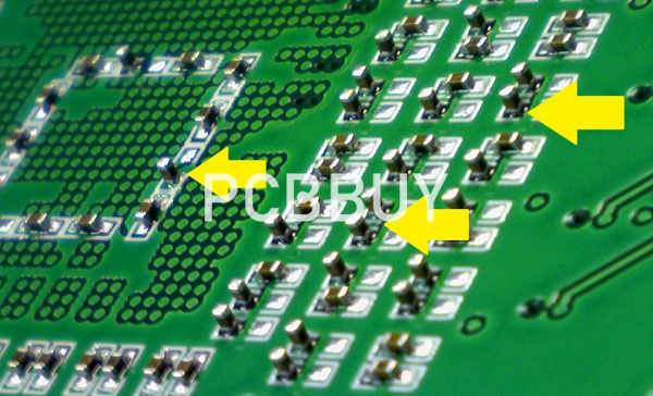
Take a simple SMD resistor as an example, which has two pads. In an ideal process, the solder will attach itself to both pads and complete its wetting process at the same time on both ends. No tombstoning issues here. But you run into a problem when the wetting process of solder is unbalanced. Like when the solder on one pad completes its wetting process before the other, which results in one side of a component solidifying while the other is still in process, and so begins the game of tug-o-war.
Of course, the wet pad ends up winning, pulling up the other pin still in the process of wetting, and the entire component gets tilted on its side, looking like a tombstone. As you can imagine, identifying exactly what caused this uneven wetting can be quite the detective work as there are so many variables in play during a typical wave reflow process. Some of the most common causes of a tombstoning issue on a PCB can include:
· The temperature of the reflow oven being uneven, which can cause the solder to begin and finalize its wetting process at different times on your PCB layout.
· Solder paste being applied to your board in a non-uniform application across all of your pads which can lead to wetting beginning and ending at different times.
· There’s also the varying sizes of pads themselves, with SMT pads having their own set of tolerances that are often ignored but can affect the accuracy of solder applications.

How to prevent tombstone effect?
One day you might get a call or an email from your manufacturer saying that you have an issue with tombstoning on your PCB. And then you’ll probably sit there with a puzzled look on your face. What the heck is tombstoning you’ll ask, and why are you calling me about it?
Tombstoning is just one of many issues that can occur during the soldering process when all of your components get attached to a bare board. And since the beginning of PCB manufacturing, tombstoning has been and continues to be an issue. While a bunch of articles on the web point the fingers of blame at manufacturers for tombstoning issues, the truth is you also have a part to play as well. So let’s dispel once and for all what tombstoning is, and what you as a PCB designer can do to prevent it at design time.
What Can I Do About This Problem?
So now you understand tombstoning, and what it looks like on your PCB design. But you might be saying to yourself – everything I just read above sounds like an issue with the manufacturer’s process, so isn’t this their problem? Well, Yes and no.
While many of the causes of tombstoning are directly related to manufacturing imperfections, there are still some factors that you can influence. Like making a mistake on pad dimensions when creating a part, or using a tombstone loving PCB finish. Here are our top five tips that you can implement in your very own design process to lessen the chance of tombstoning:
Double Check Your Component Pad Dimensions
When you’re drudging through the process of creating your own parts, it can be easy to mess up your pad dimensions without realizing it. This could be a simple mistake like making the pad dimensions too small or too large or making one pad larger than the other. Whichever mistake happens, that extra copper is going to act as a heat sink during your wave soldering process, causing one side of your pad to complete this wetting process earlier than the other.
To solve this, always make sure that you make your component footprints according to the exact specifications in your manufacturer’s datasheet. There’s no good reason to make component pads larger than necessary. The next time you make a footprint, try using this IPC-7351B calculator which can help you to precisely calculate land patterns based on exact component dimensions.
Consider Using a Different PCB Finish
If you’re working with tiny component sizes, like 0402 or 0201, which are known for tombstoning problems, then consider using an alternative to the traditional Hot Air Solder Leveling (HASL) on your board. While an HASL finish is the industry norm thanks to its low cost and wide availability, it’s also prone to causing uneven surface finishes, which can impact the solder wetting process on your components. There are several other board finishes you can consider using depending on your design constraints, like immersion tin, immersion gold, or OSP.
Pay Attention to Your Component Placement and Routing
The chances are that different trace widths on two sides of a component haven’t been that big of a deal for you to consider, but with the risk of tombstoning on tiny component packages, it is. When working with these smaller components, carefully inspect both your component placement and routing to ensure that all of the traces connecting to your pads are equal in width. It’s also a good practice to connect traces in a similar orientation, either along your x-axis or y-axis. Otherwise, you might get variable heat dissipation with differently angled traces.
Inspect the Inner Layers of Your Board for Copper Coverage
It’s not just the top and bottom layers of a board that can cause tombstoning issues. Sometimes the culprit might be hiding out in the inner layers of your board. If an inner layer of your board has a large copper area that covers only one part of a component pad but not the other, then this will most likely cause an uneven heating process during wave soldering. To prevent this, always make sure that the copper on the inner layers of your board covers both sides of a component’s pads.
Industry Category


