Transmission line in PCB
By:PCBBUY 08/14/2021 09:31

Do you know the definition of transmission line in PCB? In this passage, we will talk about the topic. If you are going to learn professional knowledge of PCB, please check and read the content we prepare below.
What is the brief introduction of transmission line in PCB?
A PCB transmission line is a type of interconnection used for moving signals from their transmitters to their receivers on a printed circuit board. A PCB transmission line is composed of two conductors: a signal trace and a return path which is usually a ground plane. The volume between the two conductors is made up of the PCB dielectric material.
The alternating current that runs on a transmission line usually has a high enough frequency to manifest its wave propagation nature. The key aspect of the wave propagation of the electrical signals over a transmission line is that the line has impedance at every point along its length and if the line geometry is the same along the length, the line impedance is uniform. We call such a line a controlled impedance line. Non-uniform impedance causes signal reflections and distortion. It means that at high frequencies, transmission lines need to have a controlled impedance to predict the behavior of the signals. Read our post: why controlled impedance really matters?
What are the types of transmission line in PCB?
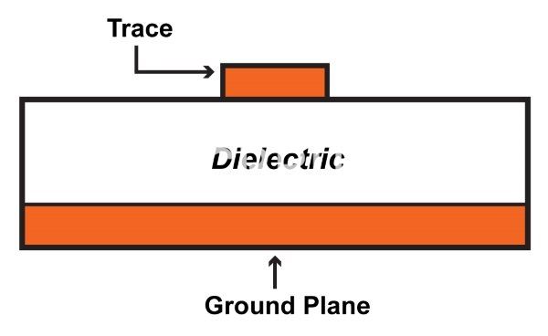
There are usually two basic types of signal transmission line interconnects used in PCBs: microstrip and stripline. There is a third type – coplanar without a reference plane but it is not very common in use.
A microstrip transmission line is composed of a single uniform trace – for the signal – located on the outer layer of a PCB board, and parallel to a conducting ground plane, which provides the return path for the signal. The trace and the ground plane are separated by a certain height of PCB dielectric. A stripline is composed of a uniform trace – for the signal – located on the inner layer of a PCB. The trace is separated on each side by a parallel PCB dielectric layer and then a conducting plane.

In addition to conventional microstrip and stripline described above, a coplanar waveguide structure has the signal trace and the return path conductor on the same layer of the PCB. The signal trace is at the center and is surrounded by the two adjacent outer ground planes; it is called “coplanar” because these three flat structures are on the same plane. The PCB dielectric is located underneath. Both microstrip and stripline may have a coplanar structure.
When is an interconnection to be treated as a transmission line?
Line inductance – The current flow in the transmission line induces the magnetic flux.When the current in the transmission line changes, the magnetic flux also varies due to which emf induces in the circuit. The magnitude of inducing emf depends on the rate of change of flux. Emf produces in the transmission line resist the flow of current in the conductor, and this parameter is known as the inductance of the line.
Line capacitance – In the transmission lines, air acts as a dielectric medium. This dielectric medium constitutes the capacitor between the conductors, which store the electrical energy, or increase the capacitance of the line. The capacitance of the conductor is defined as the present of charge per unit of potential difference.
Capacitance is negligible in short transmission lines whereas in long transmission; it is the most important parameter. It affects the efficiency, voltage regulation, power factor and stability of the system.
Shunt conductance – Air act as a dielectric medium between the conductors. When the alternating voltage applies in a conductor, some current flow in the dielectric medium because of dielectric imperfections. Such current is called leakage current. Leakage current depends on the atmospheric condition and pollution like moisture and surface deposits.
When the signal frequencies (in case of analog signals) or the data transfer rates (in case of digital signals) are low (less than 50 MHz or 20 Mbps), the time it will take for a signal to travel from its source to its destination on a multilayer PCB would be very small (< 10%) compared to the time period of one-fourth of a wavelength or the fastest rise time of a digital pulse signal. In this case, it is possible to approximate interconnect by assuming that the signal at the destination follows the signal at its source at the same time. In such a low-speed scenario, the PCB signal can be analyzed by conventional network analysis techniques and we can ignore any signal propagation time or transmission line reflections, etc.

How to analyze a PCB transmission line?
Basically, high-speed or high-frequency signals generate electromagnetic fields around them during their travel along a transmission line, and their behavior is best analyzed using Maxwell’s electromagnetic equations and the theory of electromagnetic wave propagation. In this method, we have to deal with electric and magnetic fields instead of the usual voltages and currents. The voltage between the signal line and its return path will generate an electric field and a current in the conductors, which in turn will create a magnetic field around them. Thus, voltage, current, and electric and magnetic fields all travel as waves along the transmission line.
Industry Category


