Which Is Better: Core Via VS Microvia in PCB Manufacturing?
By:PCBBUY 02/10/2022 09:16

The “simple board” is complete except for the lack of soldermask and silkscreen. The core will be at least two layers but often more. We talk about core and prepreg materials but this is a slightly different definition of ‘core’ than that. Our core can be two layers in which case there are overlapping definitions. We would still call it a core even when it is a core plus additional layers of prepreg.
In this passage, we are going to tell you everything about the differences about core via and microvia. Please check and read the content below for more information.
What is core via in PCB?
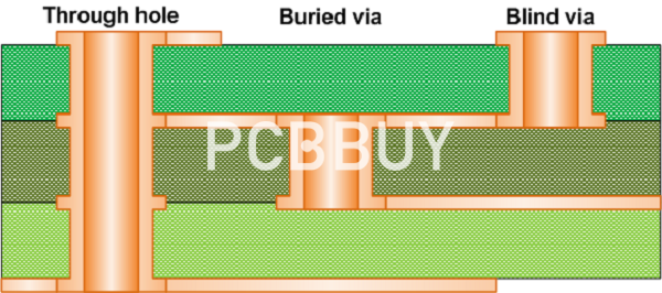
Emphasize the fact that a core via starts as a through-hole via, the same process of plating up is required to deposit copper in the hole. This translates to using the larger minimum air-gaps and line-widths consistent with what is found on the outer layers vs. typical inner-layer constraints.
Knowing that the thicker copper favors the wider geometries, it makes sense to dedicate these layers to power and ground nets who happen to also benefit from the thick copper and wide geometry. Naturally, the layers in between are the candidates for fine line routing.
When the layer count gets hectic, there are bound to be multiple sub-boards that are piled up such that core via spans are more like local elevators from a routing perspective. Grouping busses and associated power domains into dedicated sections will keep the cross contamination down on these epic high layer-count boards.
What is Microvia in PCB?
Usually, vias that are under 150 microns are known as Microvia. In the PCB design, the designers prefer Microvia because of the small size of the hole, which consumes far less space on the board than the holes that require more drilling. The layers are connected to one another with copper plating in Microvia. In some cases, a microvia will penetrate two whole layers. The blind vias that fit this description are known as skip vias. However, skip vias are not recommended by manufacturers because the nature of the hole can result in complications with plating.
In the PCB manufacturing process, microvia are drilled by lasers and have a smaller diameter compared to the standard through-hole vias. And we divide microvia into 2 types - stacked vias and staggered vias according to the location in the PCB layers.
Microvias reduce the layer count in printed circuit board designs and enable higher routing density. Microvias improve the electrical characteristics and also allow miniaturization for higher functionality in less space. It makes room for large pin-count chips that can be found in smart phones and other mobile devices. Besides, there is another type of microvias called skipvias. Skipvias skip one layer, meaning, they pass through a layer making no electrical contact with that specific layer. The skipped layer will not form an electric connection with that via. Stacked vias are piled on top of one another in different layers and staggered vias are scattered in the different layers. And they are more expensive.

How to choose core via and microvia?
The PCB manufacturing process is an expensive process. This process becomes far more costly when you need to create complex circuitry. So it is a fact that each layer in the circuit boards costs a lot. Therefore, when layers increase, the cost of the circuit board will increase.
So you can utilize microvia to replace the conventional through-hole vias. Through-hole is a very common terminology. It means normally when we talk about vias, we are considering through-hole vias.
What would happen if you replace through-hole vias with micro vias? It will decrease the number of layers which means reducing the manufacturing costs.
Besides this, a minor replacement can’t only cut decrease the cost. But also enhance the electrical characteristics of the PCB. In the age of technology, people go with the smaller and lighter devices. Therefore, high density and multilayer circuit boards are the need of this era.
Besides functionalities, microvia utilizes the minimum space of the board. Furthermore, they come in just two are three layers. So the manufacturer gives priority to these vias.
In addition to this, micro vias are available in a wide variety of patterns and materials. It makes this technology one of the finest choices of complex circuit boards. Such as staggered, via in pad and non-conductive are some of the examples. It further includes staked, offset and copper-filled material.
You can boost routing across multiple layers by using stacked micro vias in those applications requiring more than three layers. Furthermore, it also gives a built-in thermal regulation.
Industry Category


