Why HDI PCB is Popular?
By:PCBBUY 10/23/2024 17:21
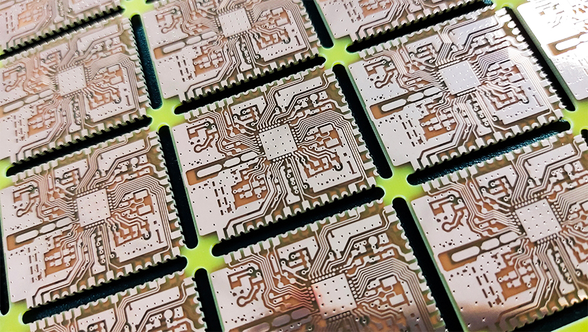
High-Density Interconnector (HDI) PCBs have become increasingly popular in modern electronics due to their advanced features and capabilities. As electronic devices continue to evolve, the demand for more compact, efficient, and reliable circuit boards has skyrocketed. This article explores the reasons behind the growing popularity of HDI PCBs, examining their unique characteristics, advantages, manufacturing processes, and applications.
What is HDI PCB?
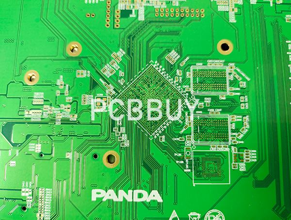
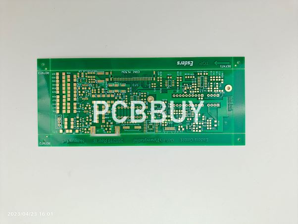
HDI PCBs are printed circuit boards with a higher wiring density than conventional PCBs. They utilize advanced manufacturing technologies such as microvias, laser drilling, and stacked vias to achieve a compact design that accommodates more components in a smaller space.
What Are Characteristics of HDI PCBs?
1. Microvias: Small vias that allow for increased density.
2. Layer Stacking: The ability to stack multiple layers of circuitry.
3. Thin Traces: Reduced trace width and spacing for compact layouts.
What Are Key Advantages of HDI PCBs?
1. Higher Wiring Density
HDI PCBs can achieve a wiring density of up to 50% more than traditional PCBs. This increase allows for the placement of more components in a limited area, crucial for modern devices.
|
Type of PCB |
Wiring Density (Components per mm²) |
|
Standard PCB |
0.5 |
|
HDI PCB |
0.75 |
2. Smaller Size and Lightweight
The miniaturization of electronic devices has led to the increased use of HDI technology. With the ability to fit more components in less space, HDI PCBs are essential for smartphones, tablets, and wearables.
3. Improved Electrical Performance
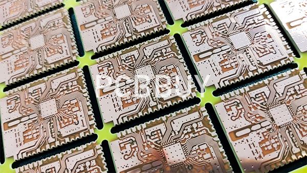
HDI PCBs offer superior electrical performance due to shorter interconnections, which reduce signal loss and improve integrity. The reduced length of traces minimizes resistance and capacitance, enhancing overall performance.
Chemical Equation:

Where Z is the impedance, R is resistance, L is inductance, and C is capacitance.
4. Enhanced Thermal Management
The materials and construction of HDI PCBs allow for better heat dissipation. By utilizing thermal vias and advanced materials, HDI PCBs manage heat more effectively, which is critical in high-performance applications.
5. Cost-Effectiveness in High-Volume Production
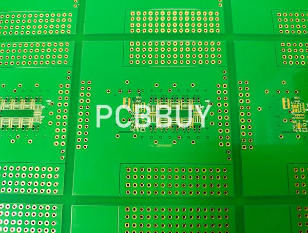
While the initial costs of HDI PCBs may be higher, they are often more cost-effective in high-volume production due to reduced material waste and lower assembly costs.
What Is HDI PCB Manufacturing Process?
1. Design Considerations
Designing HDI PCBs requires specific considerations, such as layer counts, via sizes, and material selections. Software tools like Altium Designer and Eagle are commonly used.
2. Material Selection
Materials for HDI PCBs must have low dielectric constants to enhance performance. Common materials include FR-4, Rogers, and PTFE composites.
3. Production Techniques
Laser Drilling: Allows for precise microvia creation.
Plating: Involves the electroplating of copper in the vias.
What Are the Applications of HDI PCBs?
HDI technology is prevalent in various industries, including:
Consumer Electronics: Smartphones and tablets.
Medical Devices: Portable diagnostic equipment.
Automotive: Advanced driver-assistance systems (ADAS).
Conclusion
The increasing popularity of HDI PCBs can be attributed to their numerous advantages, including higher density, smaller size, improved performance, and cost-effectiveness. As technology continues to advance, HDI PCBs will play a crucial role in the development of the next generation of electronic devices.
References
- IPC-2226: Standards for HDI PCB Design
- “Understanding High-Density Interconnector Technology” - Journal of PCB Engineering
- “Thermal Management in HDI PCBs” - Electronics Cooling Magazine
Industry Category


