Why Use Silkscreen PCB & How to Process It?
By:PCBBUY 03/30/2022 09:55

With technological advancement, the text and beautification images can also be part of silkscreen artwork design. However, the pitfall is that you may overlook the fundamental purpose of the design and may make the information unreadable easily. If you are going to learn more information about silkscreen PCB, please check and read the content below for process knowledge.

What is the importance of PCB silkscreen?
Though the Silkscreen has nothing to do with the functionality of the Printed Circuit Board, the PCB Silkscreen provides information on
· Warning Symbols – The warning symbols indicate the parameters on the high voltage points that you need to avoid or handle.
· Polarity Indicators – It helps you to trace the polarized component’s orientation.
· Locating the parts via reference designators
· It helps in identifying the test points and unique numbers for each board.
· Reference indicators – It helps in identifying the component types via BOM. The Pin 1 indicator helps you to connect the pins to the suitable pads in the footprint. The leading pattern of the component outline would show the placement of a component. The polarity indicators provide you with the polarized component’s orientation
· Pin 1 indicator – It indicates the connection of pins on the correct pads of the footprints.
· Component Online – It enables you to place the components on PCB through indications.
What are the considerations for PCB silkscreen design?
As discussed earlier, using a silkscreen PCB layout is an important aspect of board design and not including it can cause serious problems for PCB assembly and testing. The silkscreen is also used for labeling, which may include manufacturer information, testing certifications, model or serial numbers. In order to be effective and useful, the silkscreen must have clearly readable text, provide sufficient image resolution and, most importantly, be accurate. Here are a few tips to help you ensure that your silkscreen PCB layout can be used for its important roles in PCB assembly, testing and identification:
· Only use fonts approved by your CM as some fonts, although easily created in software, are difficult to generate during board manufacture.
· Use white or black instead of other colors to provide the best contrast with your board’s solder mask color.
· Make sure to follow your CM’s clearance and dimension guidelines. This will ensure that your silkscreen items do not get covered by components and are easily visible.
What are the considerations of PCB silkscreen?
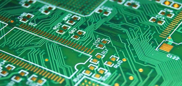
Before a circuit board is installed in a product, it must be assembled and tested first. Some of this work may be done manually, and for the technicians doing this work to find specific components, they need to be labeled. Even after the board is completed, there may still be maintenance, setups, or even field repairs that require simple information printed on the circuit board. This is accomplished with an ink that is silkscreened onto the board.

These silkscreen markings are laid out in the PCB design CAD system along with the rest of the board, and the completed artwork is usually referred to simply as the silkscreen. It is important that the correct data be included on the silkscreen, and that the correct sizes and shapes be used, as well. If these sizes are too small, or the wrong font is used, it may be unreadable.
The data you should put into your silkscreen will usually include the following:
Reference designators: Each component and assembled part on the board should have a unique reference designator.
Component symbols: While most components may have a simple rectangle or line to show how they are aligned on the board, some, such as diodes, may require more complex symbols to designate their orientation.
Pin markings: Many components will need their first pins marked, and in the case of large components like connectors with hundreds of pins, there may be additional markings as well.
Special markings: In some cases, a silkscreen may contain specific user instructions, such as switch settings or assembly instructions.
Documentation: Silkscreens are also used for marking information, such as company names and contact information, the board name and part number, bar codes, copyright, and other legal information.
Industry Category


