Why We Need to Use Software to Process PCB Panelization?
By: PCBBUY 12/14/2023 11:34

Panelizing boards is something most of us won’t have to do often. Really, you only want a panel of boards when you’re manufacturing something. For small-scale production and prototypes, bare boards will do just fine. Simply by virtue of the fact that panelizing boards is far less common than throwing some Gerbers at OSH Park or Seeed, there aren’t many utorials, and even fewer tools to do so. This is how you panelize boards quickly and easily using Open Source tools.
Are you searching for the software for PCB Panelization? If you are looking for the information of software for PCB Panelization, please check and read the content below in this passage.
Why We Need to Use Software to Process PCB Panelization?
Improves efficiency of the SMT assembly
The more the number of PCB unit boards contained in a panel, the lesser the time required for one PCB to run in orbit and transfer. This also leads to a higher rate of utilization of the pasting equipment. This can improve the SMT’s production efficiency greatly.
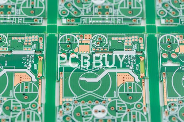
Improves the SMT production quality to prevent any bad issue during the process of production
The distribution density of the PCB components is big. Some components like edge connectors outline could be beyond the printed circuit board’s edge.
Prevents damage and it can be operated with ease
The design of the PCB panel is done to facilitate the production line’s operation. A PCB assembly has to pass through so many steps. Your semi-finished PCB or finished PCB should be placed into your turnover box. These PCBs will further be transferred, kept, and also transported through the turnover rack. To carry out these operations, there’s a need for a unique process edge. This helps in preventing damage from coming to the components present on the board of the PCB.
What is the main software for PCB Panelization?
There are several PCB panelization tools available. The two main tools for PCB panelization is altium designer and KiCad. Let’s discuss them further.

Altium Panelization
Altium Designer is one of the best software for PCB panelization. Circuit boards are available in different sizes and shapes. PCB manufacturers must be careful to carry out PCB Panelization carefully. Altium panelization tools are specifically designed to carry out your panelization tasks effectively. This software includes a lot of features for panelization. Here, we will discuss how to perform altium panelization.
You need to decide the size and shape of your PCB before getting started with Altium designer. After that, your blank PCB should be ready as you will be working with it in your layout. You will have to visit File, then click New, and choose PCB. You will have to give your project a name. Then, you have created the PCB. You can now commence work on your board outline.
KiCad Panelization
KiCad panelization is not as difficult as you think. A new script (python-based) exists which helps in panelizing KiCad circuit boards. Jan Mrazek is in charge of this project referred to as KiKit and functions well on the .kicad_pcb files, and helps in arranging them on a grid, with the v-cuts or mousebites you prefer. This is necessary for board’s separation when the production of the boards is complete.
When you work with a smaller board, the common practice is grouping them together into panels. By doing so, you are speeding up the assembly of the printed circuit board. This is because multiple boards may have the application of the solder paste, pass through the pick and place machine, and then sent as one unit to the reflow oven.
This is usually done manually. However, most of the time this script saves you much time while giving you the desired results. Using this KiKit, it is possible to gang up about six boards at once, making use of mousebites in keeping them all together all through the production process. However, it still ensures easy separation when you’ve soldered all its components.

What are the tips of PCB Panelization?
Here are some guidelines for determining how Bay Area Circuits panelizes parts:
· Multilayer (3 or more layers) PCBs are only printed on 12”x 18” panels or larger.
· To be conservative, plan for a border (or spacing) of 1 inch around the border of the panel. However, depending on the design the spacing or panel margin for 2 layer boards can be as little as 0.50 inches and 0.75 inches for multilayer boards. The spacing between boards should be 0.1 inches or 0.2 inches for round boards.
· It is highly recommended that the total yield is greater than your desired quantity. This is to account for any possible board failures that may occur during manufacturing.
Industry Category


