Why We Use Via in PCB?
By:PCBBUY 08/24/2021 09:49

Vias in PCB are very important to PCB manufacturing and they will affect the performance and quality of finished boards. If you are curious about why we use via in PCB, please check and read the content we provide for more information.
What is the importance of PCB via?
Before a PCB layout designer can start dropping vias into their board design, there are a few more details about vias to be discussed. We’ve already talked briefly about the difference in the manufacturing costs between a thru-hole via and a microvia, which can be a real wake-up call if you aren’t prepared for it. Now, here are some other considerations to keep in mind as well.
Signal Integrity
Although a via is very short, it is still a measurable length of the conductor which could cause problems with tight signal integrity requirements. For instance, a thru-hole via that connects the top two layers in a ten layer board will have 8 layers of unnecessary metal in it that could create interference. It is important to find problems like these and remedy them with techniques such as back-drilling the via to remove the unused metal from the line before it acts as an antenna. Here is where the signal integrity analyzers of PCB design tools like Cadence Allegro can be very helpful to the designer in finding these problems before the board goes out for manufacturing.
Routing Density
In situations where dense areas of the board are being routed, the designer must take care that they don’t block up routing channels or ground plane return paths with vias. This can happen under dense parts like high pin-count BGAs where there are hundreds of vias in one small area. This is where the use of blind vias and microvias becomes essential in planning out the BGA escapes so that every pin gets routed but important routing channels and planes are not blocked off under the part.

Aspect Ratio
When using a mechanical drill to create a standard via, it is important to remember that the smallest acceptable drill size is based on how thick the circuit board is. Mechanical drills have a limit to how much material they can drill through before they become unreliable. This is measured by the relationship of board thickness to drill size, and PCB fabricators will usually require an aspect ratio of no more than 10:1 for their drill sizes. This means that for a circuit board that is 62 mils thick, the smallest mechanical drill size that you should use is 6 mils or 0.006 inches. If you need a hole smaller than that, you should look into using microvias which have an aspect ratio of 1:1.
Annular Ring
The size of the via pad is important. You need to ensure that a large enough annular ring remains after the via is drilled. A mechanical drill will wander a little while it is drilling, and without a sufficient annular ring, the via may be compromised by drill breakout.
What are the main types of PCB vias?
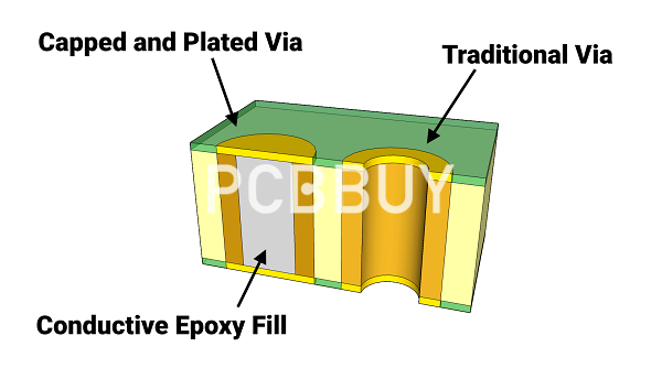
Technically, a via is a plated hole that connects copper traces between various PCB layers. Vias are what make multilayer PCBs routing possible. To make a via, the manufacturer drills a hold on the PCB on the spot where two or more traces overlap. The hole then goes through an electroplating process to make it conductive.
Ultimately, which type of via to use depends on the technology of the printed circuit board, the circuitry needs, and the targeted cost of PCB fabrication. For instance, a microvia is very desirable to use because of its smaller size, but that doesn’t necessarily make it the best choice. A microvia has more steps involved in its fabrication and, therefore, is more expensive compared to a mechanically drilled thru-hole via. But if you are designing a high-density interconnect board, the microvia becomes the better choice.

When vias are mentioned, the common picture is one that connects all the layers between the top and bottom of the PCB or through-hole vias. While most PCB designers are familiar with through-hole vias, there are other types of vias that can be handy in design.
Blind vias are a type of via that starts from the outer layer but ends in one of the middle layers. Only one part of the via can be seen on the PCB. Buried vias start and end between the inner layers of the PCB. Both blind and buried vias offer more space for routing and are favorable for HDI PCBs.
Vias are usually drilled with machines, and therefore, there’s a limit in how small they can get. Laser-drilled vias or micro vias have much smaller dimensions and is a popular approach in high-density designs.
How to determine the right vias of PCB?
To avoid PCB issues, it is important that you state your via requirements for TYPE and TREATMENT clearly in your fabrication documentation so that you get what you expect. In all cases, provide a separate file for each set of vias used in the design.
· For TYPE, supply your fabricator with the following information:
· Via type (through, blind, or buried)
· Via diameter (we recommend between 0.008” - 0.020”)
· Tolerance (+/-0.003” typical, although small or plugged vias may be +000/-hole diameter)
· Layer pairs to be connected by each drill file, if blind or buried.
Industry Category


