Why copper is used in PCB?
By:PCBBUY 05/27/2021 18:02

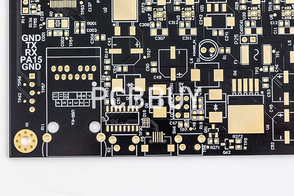
PCB is made up of several layers, including the substrate, traces, solder mask, and silkscreen. The traces are a crucial element, because they carry the electrical signals to different components across the board. Without the traces, the PCB wouldn’t function. No PCB board means almost every single electrical item that transfers data wouldn’t work!
The reason for copper’s high level of conductivity is that it has only one valence electron, also known as a free electron. Such electrons can travel freely from one atom to another with very little resistance. Electrons are the fundamental particles that hold electrical charges, so free electrons are responsible for transferring electrical signals. Copper transfers these signals without losing electricity.
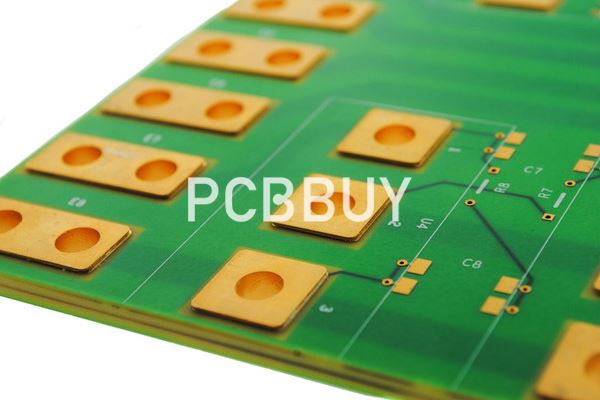
The most common element used to make traces is copper. Why is copper such a popular choice in the PCB industry? The number one benefit of copper is that it is highly conductive. This means that it can easily transmit signals without losing electricity along the way.
PCBs rely on electricity in order to perform their myriad functions. While dozens of substances can carry electric charges, copper is particularly conductive, so it has become the standard choice.
Reasons of Using Copper of PCB
There are two similar terms used in PCB design; copper balancing and copper thieving. Although they are often used interchangeably, there are some important distinctions between the two:
Copper balancing
This is the process of adding non-conductive patterns of copper to a circuit board in order to alleviate the possible bending of the board during manufacturing. PCB layer stackups that are not configured symmetrically, or individual layers with dense copper on one side versus the other, can all cause the board to warp during fabrication. Uneven copper in the board structure can also twist during the assembly process due to the excessive amount of heat used for soldering. To counter this, the PCB CAD design system will add area fills, or pours, to sparse areas of the board to copper balance the design.
Copper thieving
This is also the addition of non-conductive patterns of copper to the circuit board, but in this case, it is to even out or “thieve” some of the electrical current used for plating the board. On areas of the board where there are isolated or “lonely” traces, the current applied to the board for plating can become more concentrated on those features. This scenario may result in an under-etching of the trace giving it a “mushroom” profile instead of the clean squared edges that were expected. You can see an example of this in the image below, where the cross-section of the trace on the left depicts serious undercutting, while the trace on the right is more squared off as desired.
The mushroom shape created by the under-etching can affect both the electrical performance of the trace as well as its structural strength. By reducing the metal in the trace, the characteristic impedance of the circuit could change and thereby introducing signal integrity problems into the board. At the same time, the reduction of metal will make the trace weaker than it should be, and the mushroom shape can potentially trap acid, leading to eventual alteration and/or destruction of the trace over time.
These problems can be averted however by adding copper thieving in the areas of the circuit board where the metal is sparse. With the same amount of copper distributed throughout the board, the plating current will be applied equally and the traces will all etch the same amount.
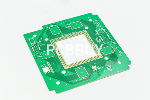
How is Copper Used in PCBs?
Copper has several uses in PCBs, from the copper-clad laminate to the traces. Copper is vital for PCBs to work appropriately.
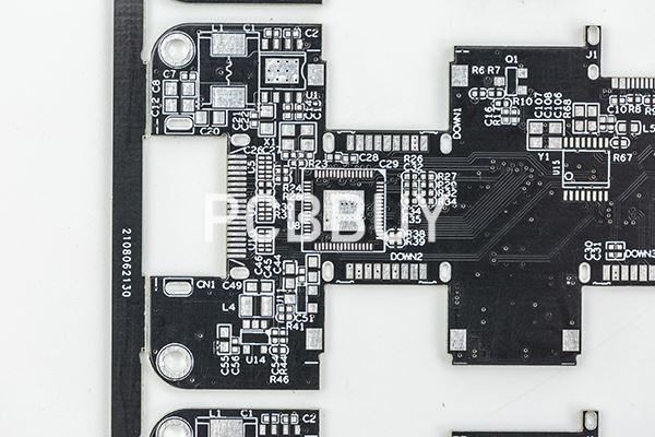
What is PCB Trace?
A PCB trace is what it sounds like, a path for the circuit to follow. The trace includes the network of copper, wiring, and insulation, as well as the fuses and the components that are used on the board.
The easiest way to understand a trace is to think of it as a road or bridge. To accommodate vehicles, the trace needs to be wide enough to hold at least two of them. It needs to be thick enough not to collapse under pressure. They also need to be made of materials that will withstand the weight of the vehicles that travel on it. But, traces do all of this to a much smaller degree to move electricity rather than automobiles.
Components of PCB Trace
There are several components that make up the PCB trace. They have various jobs that need to be done for the board to do its job adequately. Copper has to be used to help the traces do their jobs, and without the PCB, we would not have any electrical devices. Imagine a world without smartphones, laptops, coffee makers, and automobiles. That is what we would have if PCBs did not use copper.
PCB Trace Thickness
The PCB design depends on the thickness of the board. The thickness will affect the balance and will keep the components connected.
PCB Trace Width
The width of the trace is also important. This does not affect the balance or the attachment of the components, but it does keep the current transferring without overheating or damaging the board.
PCB Trace Current
The PCB trace current is necessary because this is what the board uses to move electricity through the components and wires. Copper helps this happen, and the free electron on each atom gets the current moving smoothly over the board.
Industry Category


