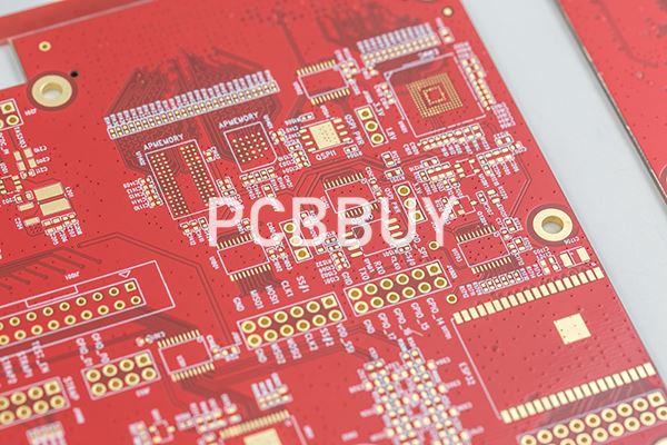
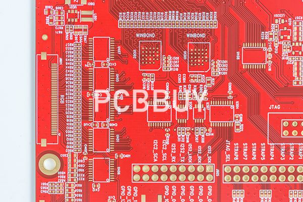
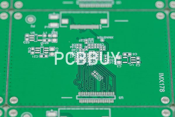
Why is Impedance important to PCB?
By:PCBBUY 05/17/2021 15:16

What is the significance of impedance to PCB circuit board? Why PCB do impedance? This article introduces what is impedance and the type of impedance first, then introduces why PCB do impedance, and finally describes the significance of impedance to PCB, please follow our contents below.
What is impedance?
In circuits with resistors, inductors, and capacitors, the resistance to alternating current is called impedance. Impedance is often expressed by Z, is a complex number, the real part is called resistance, the virtual part is called reactance, the capacitor in the circuit to the alternating current obstruction effect is called reactance, the inductance in the circuit to the alternating current obstruction effect is called inductive reactance, the capacitance and inductance in the circuit to the alternating current obstruction effect is called reactance. And the unit of impedance is ohms.
What are types of Impedance?
(1) Characteristic impedance
In computer, wireless communication and other electronic information products, the energy transmitted in PCB circuit is a square wave signal (called pulse) composed of voltage and time, and the resistance encountered by it is called characteristic impedance.
(2) Differential impedance
The driver input two of the same signal waveforms with opposite polarity, respectively transmitted by two differential lines, at the receiving end of the two differential signals subtraction. Differential impedance is the impedance Zdiff between two wires.
(3) Odd-mode impedance
Impedance ZOO of the first line to the ground in the two lines is consistent.
(4) Even mode impedance
The driver input two of the same signal waveform with the same polarity, the impedance ZCOM when the two lines are connected together.
(5) Common mode impedance
The impedance ZOE is one of the two lines to ground. The impedance values of the two lines are the same, usually greater than the odd-mode impedance.
Why do PCB boards need impedance?
PCB circuit board impedance refers to the resistance and reactance of the parameters, the alternating current blocking effect. Impedance processing is essential in PCB circuit board production. Here's why:
1, PCB line (plate bottom) to consider the installation of electronic components, plug into the consideration of electrical conductivity and signal transmission performance and other issues, so it will require the lower the impedance, the better, the resistivity should be lower than 1× per square centimeter; 10-6 below.
2, PCB circuit board in the production process to go through copper sink, electroplating tin (or electroless plating, or hot spray tin), connector soldering and other manufacturing processes, and the materials used in these links must ensure the resistivity of the bottom, in order to ensure that the overall impedance of the circuit board is low to meet the quality requirements of the product, can operate normally.
3. Tin plating of PCB circuit board is the most likely problem in the whole circuit board production, and it is the key link that affects the impedance. The biggest defect of electroless tin layer is easy to discolor (both easy oxidation or deliquation), poor brazing, will lead to the difficult welding of the circuit board, high impedance leads to poor conductivity or the instability of the whole board performance.
4, PCB circuit board in the conductor will have all kinds of signals, when the transmission rate and to raise its must raise its frequency, if the line itself due to factors such as etching, laminated thickness, wire width is different, will cause resistance to change, make the signal distortion, led to the decrease of the circuit board using performance, so they need to control the impedance value within a certain range.
Significance of impedance to PCB circuit board
For the electronics industry, according to the industry survey, the most fatal weakness of electroless tin coating is easy to discolor (both easy oxidation or solubility), poor soldering leads to difficult welding, high impedance leads to poor conductivity or the instability of the whole board performance, easy long tin must lead to PCB circuit short circuit and even burn or fire events.
It is reported that the first domestic study of chemical tin plating when the last century at the beginning of the 1990s Kunming University of Science and Technology. Then is the end of the 1990s with Guangzhou Qian chemical industry, 10 years have recognized the two organizations are doing the best. Among them, according to our contact screening investigation, experimental observation and long-term endurance test of many enterprises, confirmed that the tin layer of the same qian chemical industry is pure tin layer with low resistivity, electrical conductivity and brazing quality can be guaranteed to a higher level. No wonder they dare to ensure that its coating without any closure and anti-discoloration agent protection, can maintain a year does not change color, no foaming, peeling, permanent tin whiskers.
Later, when the whole social production industry has developed to a certain extent, many participants tend to copy each other. In fact, quite a few enterprises themselves do not have the ability of research and development or initiative. So caused a lot of products and the users of electronic products (the bottom of the PCB board or electronic products overall) poor performance, poor performance caused by the most main reason is because the impedance of problem, because when unqualified chemical tin plating technology in use process, it’s for PCB circuit board plating on pure tin is not really true (or pure metal elemental), It is a compound of tin (that is, not a metal at all, but a metal compound, an oxide or a halide, or more directly a nonmetallic substance) or a mixture of tin compounds and tin metals, which are difficult to detect with the naked eye alone... .
Because the main circuit of the PCB circuit board is copper foil, the solder joint of the copper foil is the tin layer, and the electronic components are welded on the top of the tin layer through the solder paste (or solder wire). In fact, the solder paste is welded between the electronic components and the tin coating in the melting state is the metal tin (namely, the metal element with good conductivity). Therefore, it can be simply pointed out that the electronic components are connected with the copper foil at the bottom of the PCB through the tin coating, so the purity of the tin coating and its impedance are the key; However, before connecting the electronic components, we directly use the instrument to detect the impedance, in fact, both ends of the instrument probe (or the meter and pen) are connected to the current by first contacting the tin coating on the copper foil surface at the bottom of the PCB board and then connecting with the copper foil at the bottom of the PCB board. So tin coating is the key, is the key to affect the impedance and PCB performance of the key, but also easy to be ignored the key.
As we all know, in addition to the metal element, its compounds are poor conductors of electricity or even non-conductive (this is also the key to the existence of distribution capacity or distribution capacity in the line), so tin coating in the presence of such conductive rather than conductive tin compounds or mixtures, The ready-made resistivity, or the resistivity of the electrolytic reaction resulting from future oxidation or dampness, and the corresponding impedance are quite high (enough to affect the level or signal transmission in the digital circuit), and the characteristic impedance is not uniform. Therefore, it will affect the performance of the circuit board and the whole machine.
Therefore, in terms of the current social production phenomenon, the material and performance of the coating on the bottom of PCB board is the most important and the most direct reason to affect the characteristic impedance of the whole PCB board, but also because it has the variation with the aging of the coating and damp electrolysis. So the impact of the impedance has become more recessive and variable, the main reason for its concealment is that: the first cannot be seen by the naked eye (including its changes), the second cannot be measured constantly, because it has the change with time and environmental humidity change, so it is always easy to be ignored.
Industry Category


