Why to Choose and Use PCB Microvias in Manufacturing?
By:PCBBUY 07/24/2024 16:44
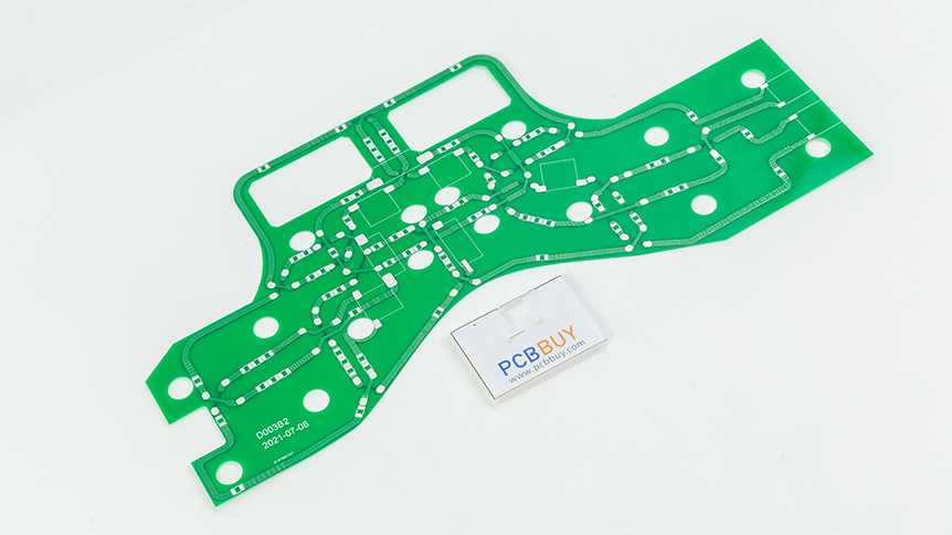
Microvias have become an essential feature in modern printed circuit boards (PCBs), enabling high-density interconnections and advanced electronic designs. This article explores the technical aspects of microvias, including their types, manufacturing processes, advantages, challenges, and applications. We provide detailed data, industry knowledge, and comprehensive tables to offer a thorough understanding of microvias in PCB technology.
What are Microvias?
Microvias are small-diameter vias used to create electrical connections between different layers of a PCB. They are typically defined by their aspect ratio, which is the ratio of the hole's depth to its diameter. Microvias generally have diameters of less than 150 micrometers and depths of less than 300 micrometers.
What Is the Importance in Modern PCB Design?
Microvias play a crucial role in miniaturizing PCBs, enabling high-density interconnects (HDIs) and improving signal integrity. They allow designers to place more components and traces in a smaller area, which is essential for applications like smartphones, tablets, and other compact electronic devices.
What Are the Types of Microvias?
Blind Vias
Blind vias connect an outer layer of a PCB to an inner layer without passing through the entire board. They are commonly used to save space on the PCB surface, allowing for more complex designs.
Advantages of Blind Vias
Space Efficiency: Allows for more component placement and routing space.
Improved Signal Integrity: Reduces the length of signal paths, minimizing signal loss and delay.
Buried Vias
Buried vias are used to connect internal layers of a PCB and do not extend to the surface layers. This type is often used in multi-layer PCBs to increase inter-layer connectivity without affecting the external layout.
What Are the Applications of Buried Vias?
High-Density Designs: Essential for PCBs with many layers and high component density.
Complex Circuits: Useful in designs that require multiple interconnections within internal layers.
Through-Hole Vias
While not a microvia in the strictest sense, through-hole vias can be miniaturized for use in HDI designs. They connect all layers of a PCB and are used in various applications requiring robust mechanical connections.
What Are the Limitations of Through-Hole Vias?
Space Consumption: Occupy significant PCB space, limiting the area available for components and routing.
Signal Integrity: Longer signal paths can lead to signal degradation.
Microvia Manufacturing Processes
Laser Drilling
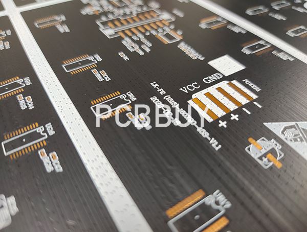
Laser drilling is the most common method for creating microvias. It uses focused laser beams to ablate the PCB material, creating precise and clean holes.
Laser Drilling Process
1. Setup: A laser drilling machine is calibrated with specific parameters based on the PCB material and the desired via dimensions.
2. Drilling: The laser beam is directed onto the PCB surface, drilling the microvia by ablating the material layer by layer.
3. Inspection: The drilled vias are inspected for accuracy and quality.
|
Parameter |
Typical Values |
|
Laser Wavelength |
355 nm (UV) |
|
Pulse Frequency |
50 kHz |
|
Hole Diameter |
50 - 100 µm |
|
Aspect Ratio |
Up to 0.75:1 |
Electroplating
After drilling, microvias are often plated with copper to establish electrical connectivity between layers. Electroplating involves depositing a thin layer of copper on the walls of the vias and the PCB surface.
Electroplating Process
1. Surface Preparation: The PCB is cleaned and treated to ensure proper adhesion of the copper layer.
2. Copper Deposition: The board is submerged in an electroplating bath, and an electric current is passed through it, causing copper ions to deposit onto the vias' walls.
3. Thickness Control: The thickness of the copper layer is controlled to meet design specifications.
|
Parameter |
Typical Values |
|
Copper Thickness |
15 - 25 µm |
|
Plating Speed |
1 - 2 µm/min |
|
Surface Roughness |
<1 µm |
Filling and Planarization
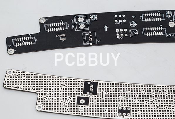
Filled microvias are used to create flat surfaces, essential for high-density designs and fine-pitch component placement. Filling materials can include conductive or non-conductive pastes.
Filling Techniques
1. Conductive Fill: Used to enhance electrical conductivity and thermal management. Commonly used materials include silver epoxy.
2. Non-Conductive Fill: Primarily for structural support and to create a flat surface for additional layers or components.
|
Parameter |
Conductive Fill |
Non-Conductive Fill |
|
Material |
Silver Epoxy |
Epoxy Resin |
|
Material |
3 - 5 W/m·K |
0.3 - 0.5 W/m·K |
|
Electrical Conductivity |
High |
Low |
What Are the Advantages of Microvias?
Enhanced Signal Integrity
Microvias reduce the length and number of signal paths, which minimizes signal loss, reflection, and crosstalk. This is crucial for high-speed and high-frequency applications.
Space Efficiency
Microvias allow for more components and traces to be placed on a PCB, enabling the design of smaller and more compact devices.
Thermal Management
Filled microvias can enhance thermal conductivity, helping to dissipate heat more effectively in high-power applications.
What Are the Challenges and Considerations?
Manufacturing Complexity
The small size and precise requirements of microvias make them challenging to manufacture. This complexity can lead to higher costs and longer production times.
Reliability Concerns
Microvias are susceptible to failure modes such as voids, cracks, and delamination. These issues can compromise the reliability and longevity of the PCB.
Cost Implications
Advanced microvia technologies, such as stacked and staggered microvias, can increase manufacturing costs. The cost must be balanced with the performance benefits they provide.
What Are the Applications of Microvias?
Consumer Electronics
Microvias are widely used in smartphones, tablets, and wearable devices, where space is at a premium, and high-density designs are essential.
Telecommunications
In telecommunications equipment, microvias enable high-speed signal transmission and are crucial for developing compact and efficient devices like routers and switches.
Automotive Electronics
Microvias are increasingly used in automotive applications for infotainment systems, advanced driver-assistance systems (ADAS), and electric vehicle (EV) power management.
Aerospace and Defense
The aerospace and defense industries use microvias in communication systems, avionics, and radar systems, where reliability and signal integrity are critical.
What Are the Future Trends in Microvia Technology?
Development of Smaller and More Complex Vias
As electronic devices continue to shrink, the demand for even smaller and more complex microvias is increasing. Innovations in laser drilling and electroplating are making it possible to create vias with higher aspect ratios and smaller diameters.
Integration with Advanced Packaging
Microvias are becoming increasingly integrated with advanced packaging technologies such as System-in-Package (SiP) and Chip-on-Board (CoB). These integrations offer significant improvements in performance and space utilization.
Improved Materials and Processes
Research into new materials and manufacturing processes is ongoing, aiming to enhance the reliability and performance of microvias. These advancements include better dielectric materials, more efficient filling techniques, and improved plating methods.
Conclusion
Microvias are a critical component of modern PCB design, enabling the miniaturization and advancement of electronic devices. Understanding the types, manufacturing processes, advantages, challenges, and applications of microvias is essential for designers and engineers. As technology continues to evolve, the role of microvias in high-density interconnects and advanced packaging solutions will only grow.
References
1. J. Coombs, "Printed Circuits Handbook," 7th Edition, McGraw-Hill, 2016.
2. R. J. Klein Wassink, "Soldering in Electronics: A Comprehensive Treatise on Soldering Technology for Surface Mounting and Through-Hole Interconnection," 2nd Edition, Electrochemical Publications, 1995.
3. IPC-6012, "Qualification and Performance Specification for Rigid Printed Boards," IPC, 2015.
4. J. H. Lau, "Advanced Microsystems for Automotive Applications 2014," Springer, 2014.
5. D. L. Green, "Fundamentals of Microvia Technology," Journal of Electronic Materials, vol. 28, no. 11, 1999.
Industry Category


