X-ray inspection system PCB
By:PCBBUY 07/17/2021 17:13

What is X-ray inspection during the PCB manufacturing? How does it work? In this passage we will focus on X-ray inspection system and provide everything about it. If you are curious about it please check the content we prepare for you below.
If you want to order PCB product, please check and custom your order online.
What is the definition of X-ray inspection?
X-ray inspection technology, also referred to as automated x-ray inspection, is a technology that can find hidden features within a target object. From the medical industry to aerospace manufacturing, x-ray inspection is a widely used method to identify manufacturing errors. It is especially prevalent in PCB inspection, as x-rays are an excellent way to test PCB quality and find hidden defects without risking damage to the board. In this guide, we’ll discuss what x-ray inspection is, how it works and what it’s benefits are, so you understand how to leverage PCB x-ray inspection for your company’s purposes.
Why X-ray inspection is popular during PCB manufacturing?
Electronics manufacturing has consistently become more sophisticated over the past several decades, with electronics in industrial, communication, military and aerospace industries advancing in ways that make inspection significantly more difficult. Some of the most significant trends that negatively affect inspection include:
· Component placement: Equipment is becoming smaller and more layered to save space and maximize functionality. As a result, many solder joints and components are being moved to inner layers within electronics, either placed between PCB layers or hidden within the final product itself.
· Component size: More circuit board components are trending toward miniaturization. With the need to create more dense boards, PCB components are expected to continue toward this trend.
· SMT: Surface mount technology makes leads and packages smaller, which has resulted in PCBs having higher density with more components hidden between layers.
The increasing density, decreasing size and more complex placement of PCBs and their components have made it nearly impossible for traditional inspection methods to find faults thoroughly. Optical, ultrasonic and thermal imaging methods are relatively ineffective due to the density of modern PCBs.
However, x-ray inspection can collect detailed images where these other methods cannot. X-ray has the ability to penetrate layers of PCB to inspect inner layers and packaging, making it more useful for inspecting the solder joints of complex PCB assemblies. For this reason, PCB inspection with x-ray technology is becoming increasingly popular.
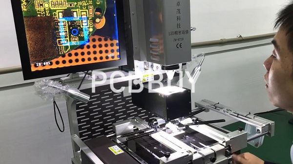
What are the working the principles of X-ray inspection?
To understand what x-ray PCB inspection is, you first need to know how x-ray inspection works. All x-ray inspection devices are made up of three basic features:
· X-ray tube: This tube has the ability to generate x-ray photons.
· Platform: The operation platform moves the sample in different directions, allowing it to be inspected from various angles and magnitudes.
· Detector: The detector on the other side of the sample catches and collects x-ray photons, converting them into an image.
X-ray imaging works using x-ray photons, which are passed through a material and collected on the other side. The x-ray photons pass through materials differently based on their physical properties, including atomic weight, density and thickness.
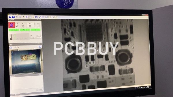
Generally, heavier elements absorb more x-ray photons, making them easier to image, while lighter elements are more transparent. Because different materials behave uniquely, differing amounts of photons are collected on the other side of the object, resulting in an image. Components in a PCB typically consist of heavier elements, making them easy to see on an x-ray image.
What are the advantages of X-ray inspection?
In x-ray images of PCBs, the metal is dark while other materials like glass, plastic and ceramics are transparent. This makes it easy to see metallic components. Combined with magnification capabilities, this allows inspectors to see various metallic parts on a board during PCB inspection with x-ray equipment. The x-ray will enable inspectors to see multiple qualities of a printed circuit and identify a range of potential problems, including:
· Solder bridges: Solder bridges are a common problem on circuit boards. This occurs when solder joints are too close or creates a connection where there should be none. These solder problems are typically hidden by other components, making them difficult to spot with optical inspections, but x-rays identify them easily.
· Solder voids: Solder voids are created when gas or flux is entrapped during soldering, often as a result of water contamination of solder paste. These voids decrease heat conductivity at the solder joint and can cause physical defects and reduced reliability. X-ray is one of the only ways to identify solder voids, so it is essential to use regularly to ensure product and process quality.
· Pin-hole fills: Inadequate pin-hole fill for through-hole connectors is a prevalent issue in circuit boards. X-ray machines can be used to identify these errors and even quantify the amount of fill missing using coordinate measurements.
One specific example of how x-ray is used is in a ball grid array (BGA) inspection. A BGA is a surface mount device that uses an array of metal spheres made of solder to make connections. This type of device is popular, as it enables high-density connections without complicating the PCB layouts. The difficulty with BGAs, however, is that the connections are made on the underside of the BGA chip. This feature, as well as the density of the solder balls, makes it difficult to solder and de-solder and increases the likelihood of forming solder bridges. The location also makes BGA chip solder joints particularly difficult to inspect. X-ray simplifies the inspection process by looking through the device to see the solder joints underneath, easily identifying bridges.
With magnification and the capability to change the viewing angle, x-ray machines can be used to find these problems and more. Even better, all of these problems may be identified during a single inspection because, unlike medical imaging, operators do not need to worry about radiation dose during operation and can use the equipment for as long as they need.
Industry Category


