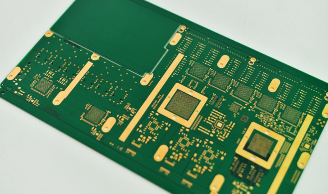
pcb etching process step by step
By: 01/18/2024 23:02

PCB etching process is one of the crucial steps in the fabrication of PCBs, and its workflow includes the following steps:
Preparation: Before initiating the etching process, it is essential to prepare the necessary materials and tools, including PCB boards, etching solution, corrosion-resistant materials, heating equipment, etc. Ensuring a clean and safe working environment is also crucial, involving wearing protective eyewear, gloves, etc.
Coating: Apply a layer of corrosion-resistant material on the PCB board to protect the areas that do not require etching. This is typically achieved by coating with photoresist. During coating, uniformity and thickness of the photoresist must be ensured to avoid undercoating or excessive thickness.
Exposure: Place the coated PCB board under ultraviolet light for exposure, causing the photoresist to harden in the exposed areas. The purpose of this step is to differentiate between the areas that need to be retained and those to be etched.
Developing: Submerge the exposed PCB board into a developing solution, dissolving the unhardened photoresist and leaving only the hardened portions visible. The goal of this step is to clearly reveal the areas that need to be retained.
Etching: Immerse the developed PCB board into an etching solution, dissolving the areas that need to be etched. The objective is to remove the unwanted portions, leaving behind only the desired areas. During etching, it is crucial to control parameters such as solution concentration, temperature, and time to ensure quality and precision.
Stripping: Retrieve the PCB board from the etching solution and remove the remaining photoresist using a stripping solution or physical methods. The purpose of this step is to make the final PCB board surface smooth and tidy.
Cleaning: After stripping, the PCB board needs to be cleaned to remove impurities and residues from the surface. The goal is to ensure the quality and reliability of the final PCB board.
If you want to order PCB product, please check and custom your order online.
In the PCB etching process, attention should be given to the following points:
l Ensure the quality and uniformity of the photoresist during coating and stripping to prevent undercoating or excessive thickness.
l Select appropriate light sources and exposure times during the exposure phase to guarantee effective hardening of the photoresist.
l Control the concentration and temperature of the developing solution during developing to prevent incomplete dissolution of the photoresist.
l Manage parameters such as solution concentration, temperature, and time meticulously during etching to ensure quality and precision.
l Choose suitable cleaning agents and methods during the cleaning step to remove surface impurities and residues.
In summary, the PCB etching process is a complex procedure that requires precise operation and management. Strict control of process parameters and quality standards is necessary at each step to guarantee the quality and reliability of the final PCB board. Additionally, enhancing quality control and testing during the production process is crucial to promptly identify and address potential issues, ensuring product stability and reliability.
Industry Category


