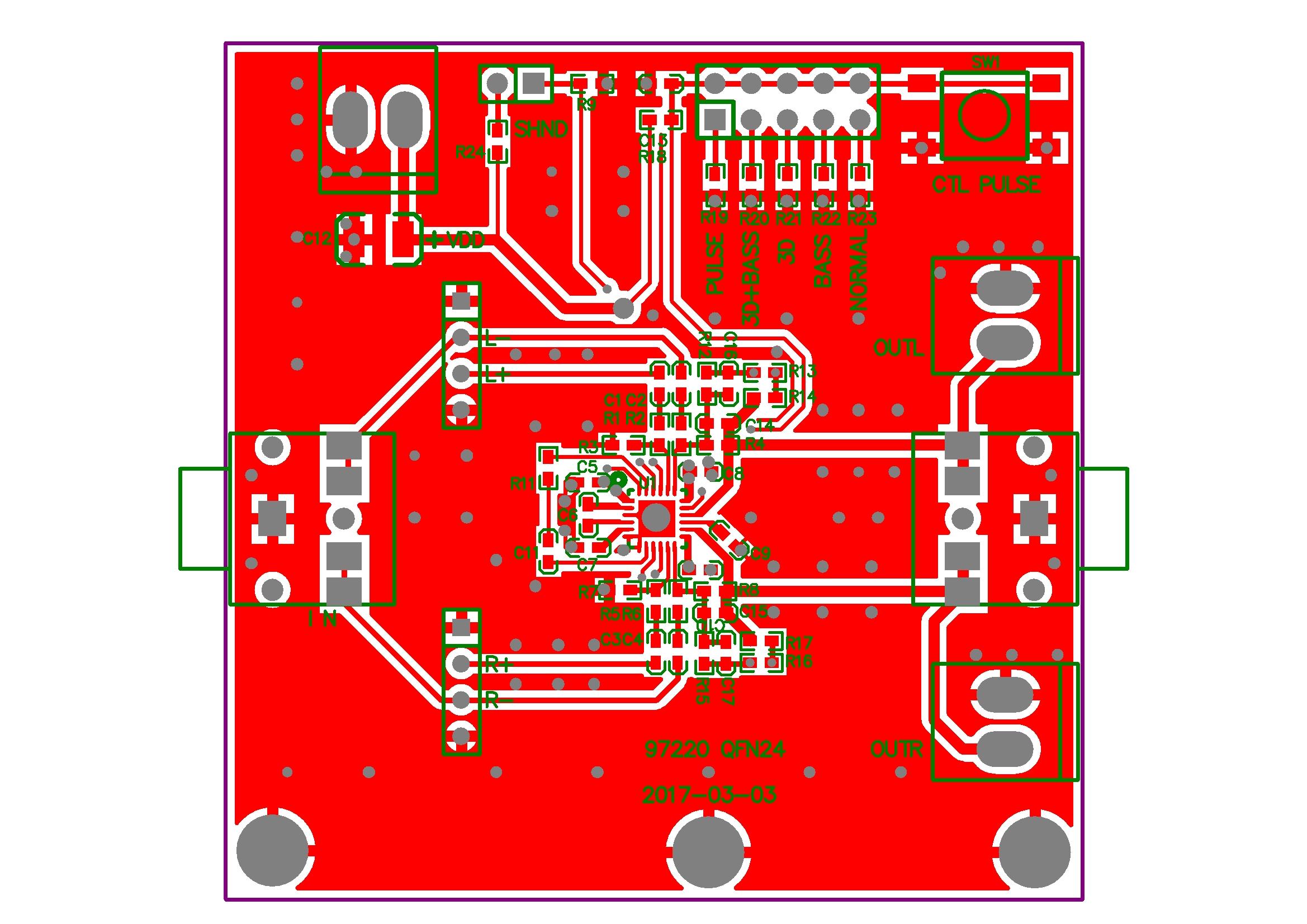
PCB layout
By:PCBBUY 04/26/2021 10:18

PCB layout, as the most basic process, transfer a circuit from a breadboard to a more stable and permanent physical form. As a link in the design process and also a very important link, In the case of reasonable hardware circuit design, it is actually an absolutely important index that affects performance.
PCB layout is a very advanced engineering tool for board design with intelligent manual routing of high-speed and differential signals, shape-based auto router, advanced verification, and wide imports and exports capacity. Of all the PCB manufacturing process, PCB layout is a very important step and preparatory work to complete the product design.

If you want to order PCB product, please check and custom your order online.
Usually, PCB layout provide following features below:
1) Smart project structure
2) Placement features
3) Manual routing
4) Advanced verification features
5) 3D PCB preview & STEP export
Know about PCB layout guidelines
Since PCB is the key point of the matter, the layout is pretty critical before the whole manufacturing process. To protect against shorts and other damage, specific layout steps should be taken.
Structure of PCB
Before PCB layout, it is necessary to know the basic structure of PCB.
1) Base: The base material is most often made from fiberglass or glass epoxy fibers. FR4 is the most commonly used such material, but there are other options available depending on your project and other factors. One example is high-temp resistant plastic. A solid base is used to help ensure that the PCB is rigid and can hold components. With that being said, board thickness can vary dramatically from one application to another, ranging from 0.8mm to as thick as 1.6mm or even more in some cases.

2) Components: A very broad range of components will need to be integrated with the PCB, including resistors, and numerous others. The number of components and their relative size will determine the size of the board, as well, although some techniques can be used to reduce the size, such as miniaturization, as well as creating double-sided PCBs and multilayer PCBs. These latter two options help you condense what would be very large PCBs into a footprint that is a fraction of the size.
3) Copper: Copper is used with most PCBs, and is the metal through which electrons flow, powering the components and, ultimately, the device in which the PCB is installed. Copper may be layered directly onto the board in varying thicknesses, or copper foil may be applied instead, depending on the needs of the project. Copper is usually measured in ounces per square foot, with the most common being one ounce per square foot. However, high-capacity PCBs can hold much more copper, up to three ounces per square foot.
Layout Rules
1) Under normal circumstances, all the components should be arranged on the same surface of the circuit board, only when the top element is too dense, can some highly limited and small calorific devices, such as patch resistance, patch capacitance, patch IC, etc., be placed in the low level.
2) Under normal circumstances, all the components should be arranged on the same surface of the circuit board, only when the top element is too dense, can some highly limited and small calorific devices, such as patch resistance, patch capacitance, patch IC, etc., be placed in the low level.
3) From the edge of the circuit board is generally not less than 2MM. The best shape of the circuit board is rectangular. When the circuit board ruler is greater than 200MM by 150MM, the mechanical strength that the circuit board can withstand should be considered.

Layout process
Components: It is necessary to set the location and orientation of components. Usually, you’ll maintain the same orientation for all components to help reduce soldering and routing errors. It also makes your board easier to install and test.
Relational Placement: In addition to directional placement, you also need to think about relational placement. In PCB layout, to leave space between components for your traces and to help reduce heat.
Routing: Routing refers to the actual placement of the traces that connect your components to each other and allow electricity to flow through the circuit. If your components are too close together, you’ll have little room for these connections.
Wanna know PCB knowledge? Check and read for more.
Industry Category


