Advanced HDI PCB Capabilities to High-Density Innovation
By:PCBBUY 06/25/2025 15:03
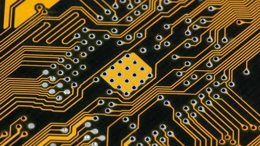
In today’s era of ultra-compact electronics and multi-functionality, the demand for advanced HDI PCB (High-Density Interconnect Printed Circuit Boards) is greater than ever. These multilayered boards are the backbone of smartphones, automotive radar systems, medical implants, and aerospace equipment.
At PCBBUY, we specialize in high-precision advanced HDI PCB manufacturing, backed by rigorous engineering, leading-edge facilities, and full-stack capabilities to serve global innovators.
What Is an Advanced HDI PCB?
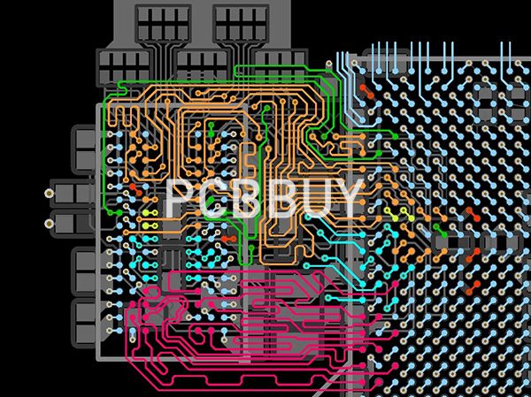
While standard HDI PCBs feature one or two layers of laser-drilled microvias, advanced HDI includes multi-order constructions such as 1+N+1, 2+N+2, 3+N+3, stacked or staggered vias, via-in-pad plating, and copper-filled microvias. These enable higher wiring density, better signal integrity, and reduced electromagnetic interference.

PCBBUY’s Advanced HDI PCB Capabilities Overview
Here’s a detailed breakdown of our production capabilities, based on our internal standards:
|
Capability |
Specification |
Remarks |
|
Material |
FR-4 |
Custom options: TG135–TG170, halogen-free, CTI-enhanced materials |
|
Number of Layers |
1st order: 4–10 layers2nd stage: 6–10 layers |
Supports progressive stack-up and multi-stage lamination |
|
Construction Types |
1st order: 1+N+1, 1+1+N+1+12nd order: 2+N+2, 1+2+N+2+1 (n buried vias ≤0.3mm) |
Via structures are customized per client documentation; electroplated filled vias available |
|
Minimum Trace Width |
2/2 mil (0.05/0.05mm) |
Designed for ultra-fine line routing using LDI imaging |
|
Blind Via Tolerance |
Mechanical ≥0.15mmLaser ≥0.075mm |
Microvias are stackable, compatible with copper via fill or resin fill techniques |
|
Hole Size |
Minimum: unilateral ≥0.3mm |
Mechanical drilling + laser micro-drilling compatible |
|
Hole Copper Thickness |
Mechanical: ≥18μmLaser: ≥13μm |
Optimized for conductivity and reliability in via structures |
|
Via Electroplating |
Depth: 0.05mm–0.1mmTolerance: ±15% |
Electroplated via filling ensures full-metal conductivity across all stacked via levels |
Manufacturing Process Flow at PCBBUY
To achieve advanced HDI PCB quality, PCBBUY implements a tightly controlled and intelligent manufacturing process:
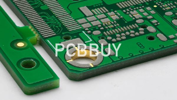
-
Stack-up Simulation & DFM Review
Our engineers simulate impedance, via positioning, and signal integrity before production begins.
-
Laser Drilling
Using CO₂ or UV laser machines, we drill microvias as small as 75μm with exacting depth control.
-
LDI Imaging
Laser Direct Imaging (LDI) allows precise fine-line exposure, supporting 2/2mil line/space designs.
-
Copper Plating and Filled Vias
Through electroplating, we fill blind vias with copper to ensure electrical continuity and thermal stability.
-
Sequential Lamination
Multi-order HDI requires multiple lamination steps—each conducted with vacuum pressure and x-ray alignment.
-
AOI + Electrical Testing
All PCBs are inspected with 100% AOI and Flying Probe or Fixture Testing to ensure functionality.
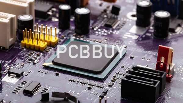
Benefits of Choosing Advanced HDI PCBs from PCBBUY
-
✅ Compact size for wearables and handhelds
-
✅ Enhanced signal transmission speed
-
✅ Excellent thermal dissipation
-
✅ Support for BGA, CSP, and Flip-Chip mounting
-
✅ Multilayer routing in limited PCB real estate
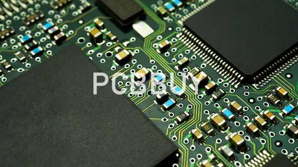
What Affects the Advanced HDI PCB Cost?
At PCBBUY, we aim for high value and high yield. Here are major cost influencers:
|
Cost Driver |
Impact on Price |
|
Layer count (e.g. 1+6+1) |
More laminations = higher processing complexity |
|
Microvia structure |
Stacked vias are costlier than staggered |
|
Via fill type |
Copper-filled > Resin-filled > Non-filled |
|
Base material |
TG170 or halogen-free increases material cost |
|
Line/space density |
2/2mil requires LDI = increased processing cost |
|
Surface finish |
ENEPIG > ENIG > HASL |
Industries We Serve with Advanced HDI
-
Consumer Electronics (e.g. smartphones, tablets)
-
Automotive (radar, LiDAR, ADAS)
-
5G Infrastructure (antenna modules)
-
Medical Devices (implantable monitors)
-
Aerospace & Defense (satellite boards)
Why Choose PCBBUY for Advanced HDI PCB Projects?
-
Global fulfillment & multilingual engineering support
-
Fast prototyping: 5–7 working days
-
Free stack-up consultation & DFM support
-
ISO9001, IATF 16949, UL certified
-
100% E-test, AOI, and QC records available
FAQ: Advanced HDI PCB Insights
|
🔎 Question |
✅ Answer |
|
What does 2+N+2 mean in HDI? |
It refers to two sequentially laminated outer layers and multiple inner layers (N) with microvias. |
|
Are stacked vias reliable? |
Yes, when copper-filled and plated correctly. PCBBUY follows IPC-6012 Class 2/3 standards. |
|
Can I use via-in-pad with advanced HDI? |
Yes, we support via-in-pad with laser drilling and copper fill. |
|
What’s the turnaround time for HDI prototypes? |
Typically 5–7 working days, depending on stack-up complexity. |
Ready to Build Your Next Advanced HDI PCB?
Contact PCBBUY today to get a free engineering consultation, or try our instant quote tool online. Let our expertise empower your product innovation.
Industry Category


