BGA Solder Joint Inspection Ensures Quality and Reliability
By:PCBBUY 10/28/2025 17:06
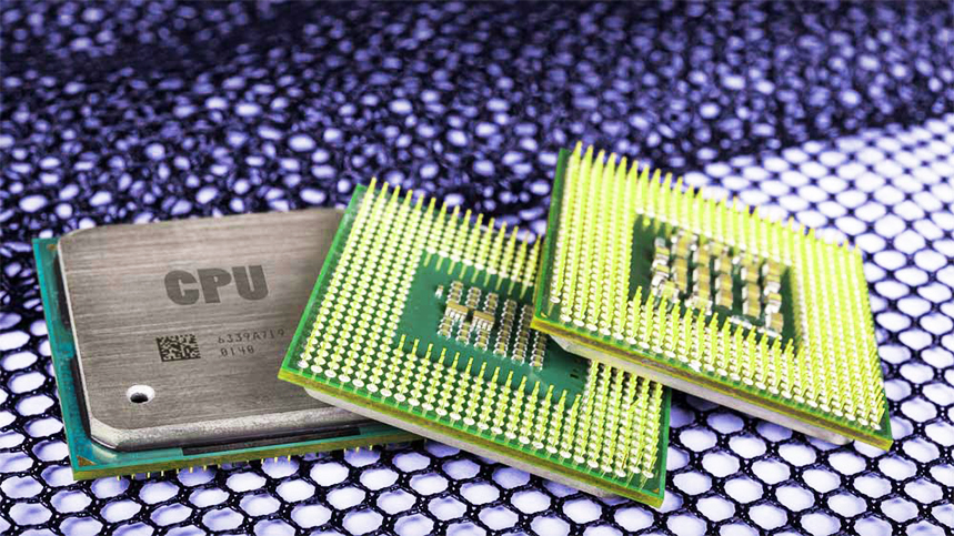
In the world of modern electronics manufacturing, BGA solder joint inspection plays a critical role in ensuring product reliability and performance. As electronic devices become smaller and more powerful, Ball Grid Array (BGA) packages are widely adopted due to their high density and excellent electrical performance. However, these components present unique inspection challenges that require advanced equipment and professional expertise.
At PCBBUY, we integrate industry-leading BGA inspection technologies into our SMT and PCBA production lines, ensuring every assembly meets the highest quality standards demanded by global customers.
Why BGA Solder Joint Inspection Is Essential
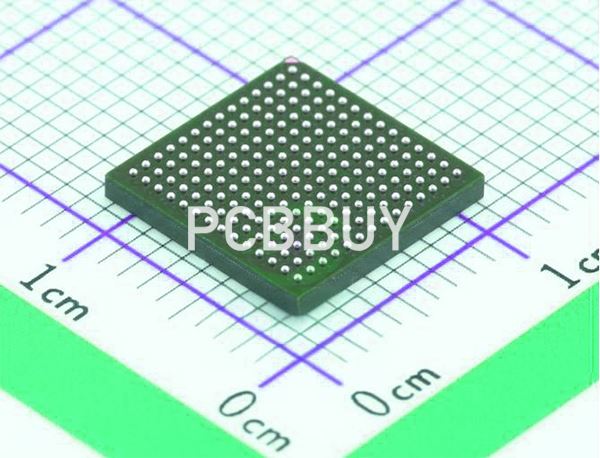
Unlike traditional leaded components, BGAs have solder balls hidden underneath the package body, making direct visual inspection impossible. Defects such as voids, bridging, cold solder joints, and insufficient wetting can occur during the reflow soldering process — and if left undetected, they can lead to serious reliability issues like intermittent connections or total circuit failure.
To address these hidden defects, BGA solder joint inspection must be performed using non-destructive methods, such as X-ray analysis, automated optical inspection (AOI), and functional testing.
Advanced BGA Solder Joint Inspection Process at PCBBUY
PCBBUY employs a comprehensive and automated inspection workflow designed to guarantee 100% quality assurance. Our BGA solder joint inspection process includes the following stages:
a. Automated Optical Inspection (AOI)
Although AOI cannot detect hidden joints directly, it helps identify surface defects such as misalignment, tombstoning, and solder bridging. PCBBUY’s AOI systems use high-resolution cameras and 3D scanning to verify solder paste deposition and component placement before reflow.
b. X-Ray Inspection for Hidden Defects
The most crucial step in BGA solder joint inspection is X-ray analysis. PCBBUY utilizes high-definition 2D and 3D X-ray systems that can visualize the internal structure of each solder joint. These systems detect voids, head-in-pillow (HIP) defects, solder ball cracks, and other anomalies with micron-level accuracy.
Our engineers analyze the grayscale contrast and solder ball geometry to assess the joint integrity and wetting quality of every BGA connection.
c. Functional and Reliability Testing
After X-ray verification, PCBBUY performs functional testing and thermal stress tests to simulate real operating conditions. These tests ensure that every BGA assembly not only passes visual inspection but also performs reliably under thermal cycling and mechanical stress.
3. Common Defects Detected During BGA Solder Joint Inspection
Through our advanced inspection systems, PCBBUY commonly identifies and corrects the following BGA-related defects:
|
Defect Type |
Description |
Impact on Performance |
|
Voids |
Air gaps within solder joints |
Reduced thermal/electrical conductivity |
|
Bridging |
Unwanted solder connection between adjacent balls |
Short circuits |
|
Head-in-Pillow (HIP) |
Poor solder fusion between BGA and PCB pad |
Intermittent or open circuits |
|
Cold Joint |
Incomplete melting during reflow |
Weak mechanical strength |
|
Misalignment |
Incorrect placement of BGA package |
Connection failure |
PCBBUY’s real-time feedback and process monitoring system allow our engineers to trace the root cause of these defects — whether it’s paste printing, component alignment, or reflow profile settings — and implement immediate corrective actions.
4. PCBBUY’s Strength in Precision and Process Control
At PCBBUY, quality assurance begins at the design stage. Our engineers carefully optimize the stencil aperture, reflow temperature profile, and solder paste formulation to minimize the risk of BGA defects before production even starts.
We also adopt statistical process control (SPC) and traceability systems to monitor each BGA assembly throughout the SMT line. Every board is logged with a unique serial number, allowing full traceability of process data and inspection images — a key factor for high-reliability industries such as automotive, aerospace, and medical electronics.

5. Benefits of Partnering with PCBBUY for BGA Solder Joint Inspection
By choosing PCBBUY, customers gain access to:
· Cutting-edge X-ray inspection technology with real-time defect mapping
· Comprehensive PCBA manufacturing services, from prototyping to mass production
· Experienced process engineers who specialize in BGA reflow optimization
· Strict IPC-A-610 and ISO 9001 quality standards compliance
· Transparent reporting and image documentation for every inspected board
These strengths ensure your PCBA projects meet not just visual quality standards, but also long-term performance and reliability benchmarks.
6. Conclusion
In today’s competitive electronics manufacturing industry, BGA solder joint inspection is not just a quality control step — it is the foundation of reliability.
With PCBBUY’s advanced X-ray systems, strict process control, and professional engineering support, customers can rest assured that every solder joint is precisely formed, inspected, and guaranteed for performance.
If you’re looking for a trusted partner who prioritizes precision and quality in every step of the assembly process, PCBBUY is your best choice.
Industry Category


