Filled and Capped Vias in PCB Manufacturing and High-Reliability Solutions
By:PCBBUY 07/22/2025 17:36
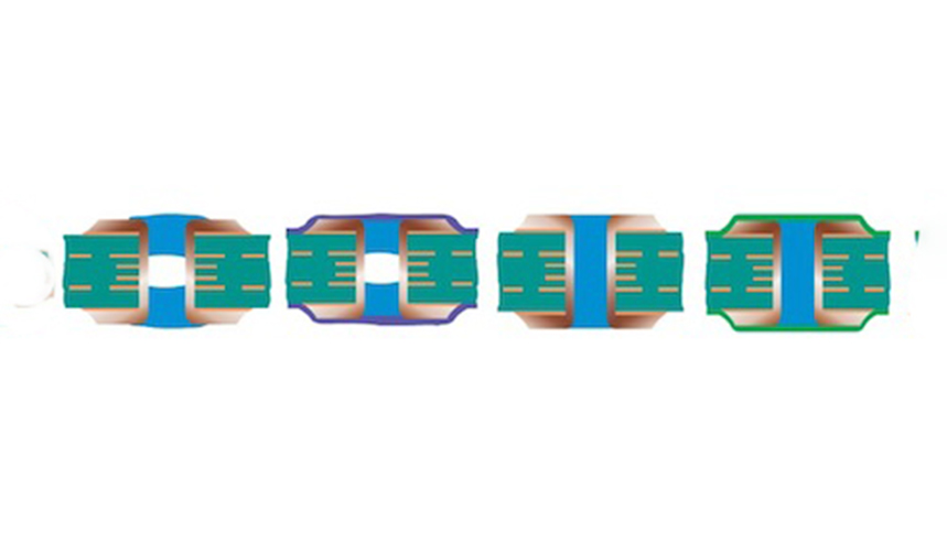
Why Filled and Capped Vias Matter
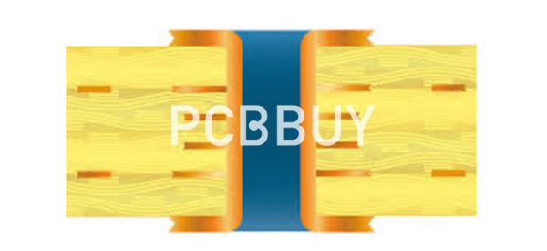
In today's high-density and high-reliability electronic designs, filled and capped vias are an essential technology for ensuring robust via structures, especially in BGA pads, via-in-pad applications, and HDI PCB designs. These vias are first filled with conductive or non-conductive epoxy, then capped with copper plating to create a flat, solderable surface.
At PCBBUY, we specialize in advanced via processing solutions—including filled and capped vias—to meet the demands of high-end industries such as telecommunications, automotive, aerospace, and medical devices.
What Are Filled and Capped Vias?
Filled and capped vias are plated-through or blind vias that are filled with epoxy and copper plated over the surface, creating a level pad. This process is crucial for:
-
Via-in-pad design
-
Improved solder joint reliability
-
Enhanced thermal and mechanical strength
-
Minimized solder wicking during reflow
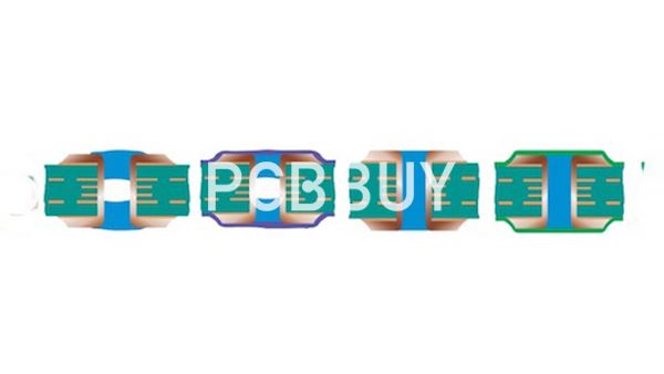
Compared to tented or plugged vias, this solution offers better surface planarity and reliability in multilayer PCBs.
PCBBUY’s Technical Capabilities for Filled and Capped Vias
Based on our internal standards and equipment, PCBBUY delivers epoxy filled via processes with precise control. Below is a summary of our key process parameters:
|
Item |
Standard |
Remarks |
|
Ink |
Zhuyou epoxy ink |
Stable performance and excellent insulation |
|
Size |
Board length ≤650mm |
Oversize boards to be evaluated individually |
|
Board Thickness |
0.2–8.0mm |
Common for HDI, rigid-flex, or multilayer PCB |
|
Plugged Via Hole Size |
0.2–1.0mm |
Oversized vias to be specially reviewed |
|
Hole Range |
Adjacent hole size difference within 0.2mm |
Ensures uniform plug filling pressure |
|
Hole Sunken Control |
Hole size ≤0.4mm: sag ≤15μm; Hole size >0.4mm: sag ≤50μm |
Zero-sag applications require re-evaluation |
This tight control of sunken depth, hole diameter, and ink quality ensures the filled via meets mechanical and thermal performance requirements, especially for critical interconnection zones.
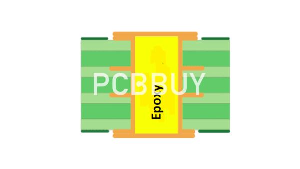
The Manufacturing Process at PCBBUY
PCBBUY follows a six-step process to ensure the quality and reliability of filled and capped vias:
-
Drilling: Via holes are precisely drilled using laser or mechanical tools.
-
Desmear & Cleaning: Removes residue and prepares the hole surface for filling.
-
Epoxy Filling: Conductive or non-conductive epoxy is filled into the vias.
-
Curing: Filled epoxy is hardened under controlled temperature and time.
-
Planarization: Excess resin is removed to ensure flat surface.
-
Copper Capping: A copper layer is plated over the filled via to create a solderable pad.
Advantages of Using Filled and Capped Vias in Your Design
-
✅ Improved SMT reliability – no dimples or solder voids
-
✅ Smooth pad surface – ideal for BGA or CSP packaging
-
✅ Stronger mechanical connection – suitable for high-stress environments
-
✅ Better thermal conduction – excellent for power PCBs
-
✅ IPC-4761 Type VII Compliant – meets international industry standards
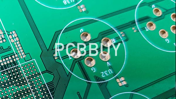
Quality Control & Testing at PCBBUY
We implement the following QA practices to ensure each via is properly filled and capped:
-
X-ray inspection for internal fill quality
-
Cross-section micro-cutting to verify epoxy spread and copper cap thickness
-
Sunken depth measurement with high-precision instruments
-
Electrical testing for interconnection reliability
Our rigorous testing ensures your via-in-pad or buried via designs are fully functional and production-ready.
Application Scenarios of Filled and Capped Vias
PCBBUY’s filled and capped via solutions are widely used in:
-
High-speed BGA routing
-
HDI PCB for smartphones and tablets
-
RF and microwave circuit boards
-
Automotive ECUs and industrial controls
-
Medical devices and aerospace systems
Why Choose PCBBUY for Filled and Capped Vias?
At PCBBUY, we offer:
-
🏭 State-of-the-art HDI production lines
-
📐 Engineering support for DFM optimization
-
🕐 Fast lead time for prototypes and mass production
-
🧪 Advanced epoxy materials like Zhuyou epoxy ink
-
🔍 Free file review to validate your via stackup design
Whether you're developing compact consumer electronics or mission-critical systems, we’re the filled and capped vias manufacturer you can trust.

FAQ: Filled and Capped Vias
Q1: What’s the difference between filled vias and capped vias?
A1: Filled vias are drilled and filled with epoxy. Capped vias are additionally plated with copper on top. Together, they ensure a flat, solderable surface.
Q2: Are filled and capped vias necessary for via-in-pad designs?
A2: Yes, they prevent solder from flowing into the via hole, ensuring strong solder joints for BGAs or QFNs.
Q3: Can PCBBUY control via sagging to zero?
A3: Yes, but controlling sunken depth to zero requires additional process evaluation and precision tooling.
Q4: What filling materials does PCBBUY use?
A4: We primarily use Zhuyou epoxy ink, which has excellent thermal and electrical properties.
Q5: Is this process IPC-compliant?
A5: Yes, PCBBUY follows IPC-4761 Type VII guidelines for filled and capped vias.
Conclusion
Filled and capped vias are no longer optional in high-end PCB design—they’re essential. With PCBBUY’s engineering expertise, epoxy fill technology, and copper capping process, we help you achieve durable, solderable, and performance-ready PCB structures for any application.
Industry Category


