Final Thoughts on HDI Flex PCB Capabilities
By:PCBBUY 06/30/2025 16:20
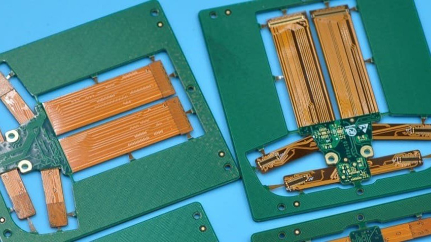
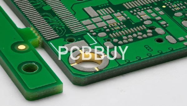
As the demand for compact, high-performance electronics grows, HDI flex PCBs (High-Density Interconnect Flexible Printed Circuit Boards) have become essential in medical, aerospace, automotive, and consumer electronics sectors. PCBBUY offers advanced HDI PCB manufacturing services that combine flexibility, durability, and precise interconnect density. In this article, we detail the manufacturing capabilities and processes of PCBBUY, highlighting how we deliver industry-leading solutions.
HDI Flex PCB Material Selection
Standard: FR-4
Custom Options: TG135-TG170, halogen-free, high CTI materials
Material selection is the foundation of HDI flex PCB reliability. At PCBBUY, we use FR-4 as the default base while offering halogen-free and high thermal endurance materials upon request. These materials undergo strict quality evaluation to support dynamic flexing and high-temperature applications, ensuring your flex boards remain stable under stress.
Layer Configuration and Flexibility Range
Standard:
-
First Order: 4-10 layers
-
Second Order: 6-10 layers
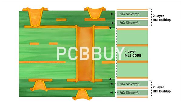
For advanced HDI flex PCBs, PCBBUY supports complex multi-layer structures. Depending on product design, we can manufacture first-order (4-10 layers) and second-order (up to 10+ layers) stack-ups. Flexible dielectric films are inserted between layers to enhance bendability without compromising electrical performance.
HDI Flex PCB Stack-Up & Construction Type
Standard:
-
1+N+1, 1+1+N+1 (blind via ≤0.3mm)
-
2+N+2, 1+2+N+2+1 (blind via ≤0.3mm)
PCBBUY Engineering Note: Based on your documentation, we prioritize internal mechanical via structures. For limited structures, we use electroplated via filling, ensuring compact design with optimal conductivity.
Minimum Trace Width and Precision Control
Standard: 2/2mil (min)
To support dense routing in wearable and miniaturized electronics, PCBBUY manufactures HDI flex PCBs with minimum trace/space of 2/2mil. Our LDI (Laser Direct Imaging) equipment ensures tight impedance control and signal integrity.
Blind Via Drilling Options
Standard:
-
Mechanical blind hole ≥0.15mm
-
Laser blind hole ≥0.075mm
To support micro-interconnections in flexible circuits, PCBBUY uses both CO2 and UV laser drilling to produce clean and reliable micro blind vias. Our processes allow smaller pad sizes without compromising connectivity.
Micro Hole Size Capabilities
Standard: Minimum unilateral hole ≥3mil
To meet ultra-fine pitch component demands, PCBBUY provides microvia formation with ≥3mil accuracy. We verify all hole sizes through AOI (Automated Optical Inspection) and cross-section analysis.
Hole Copper Thickness in Flexible Applications
Standard:
-
Mechanical hole copper >18μm (no laser via)
-
Laser via: >13μm
PCBBUY applies selective plating to balance copper thickness and flexibility. For critical flex zones, we offer thinner plated profiles while maintaining conductivity, allowing HDI flex boards to fold, twist, and stretch without cracking.
Via Filling and Electroplating Control
Standard:
-
Electroplating depth: 0.05mm~0.1mm
-
Tolerance: ±15%
Our electroplated via filling process ensures solid copper plug-in, fully metallizing the via for enhanced reliability. PCBBUY uses advanced chemical baths and agitation control to maintain consistency across batches.

Why Choose PCBBUY for Your HDI Flex PCB Needs?
-
Over 10 years of HDI flex PCB fabrication expertise
-
In-house laser drilling, LDI imaging, and automated testing lines
-
Flexible MOQ and fast lead time for prototype to mass production
-
Engineering review and one-on-one support for custom stack-up design
Quality Control and Reliability in HDI Flex PCB Manufacturing
At PCBBUY, quality control is not just a final step — it's integrated into every phase of the HDI Flex PCB manufacturing process. From incoming material inspection to multi-stage in-process quality checks, we ensure that every flexible HDI board we produce meets IPC-6013 standards. Our automated optical inspection (AOI), X-ray testing for buried vias, and electrical testing for continuity and shorts are just a few measures taken to guarantee product excellence.
In addition, our engineering team provides full DFM (Design for Manufacturability) review to optimize your design for performance, durability, and cost-efficiency. This approach reduces the risk of signal integrity issues, delamination, and mechanical stress — crucial in applications like aerospace, medical devices, and 5G mobile products.

Applications of HDI Flex PCBs
Thanks to their compact structure and ability to withstand mechanical flexing and vibration, HDI Flex PCBs are widely used in:
Foldable smartphones and tablets
Wearable electronics (smartwatches, AR glasses)
Automotive infotainment and LiDAR systems
Medical implants and diagnostic tools
Military and aerospace avionics
Industrial robots and compact IoT modules
Frequently Asked Questions (FAQs) About HDI Flex PCB
To further support our customers and website visitors, here are some common questions and clear, concise answers regarding HDI Flex PCB production and capabilities:
What materials are used in HDI Flex PCB production?
We typically use polyimide-based flexible laminates combined with FR-4 stiffeners if needed. PCBBUY also supports halogen-free, RoHS-compliant, and high-temperature TG135-TG170 materials depending on the application.
What is the minimum hole size and copper plating in HDI Flex PCBs?
Laser via holes can be as small as 0.075mm (75μm).
Minimum mechanical via size is 0.15mm.
Hole copper thickness is >13μm for laser vias, and >18μm for mechanical vias to ensure reliability.
Can PCBBUY support stacked or staggered via structures?
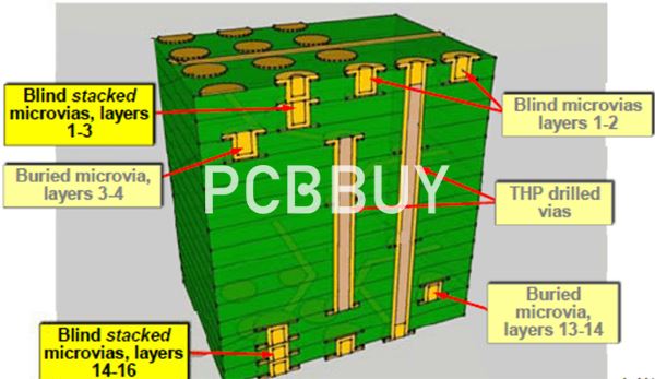
Yes. We offer multiple stacked or staggered microvia configurations, including:
· 1+N+1 and 2+N+2 structures
· Buried and blind vias
· Laser via with via filling and copper capping
How does the cost of HDI Flex PCBs compare to traditional rigid boards?
The cost of HDI Flex PCBs is generally higher due to:
Use of premium polyimide materials
Complex drilling and laser via processes
Multilayer lamination
However, for compact, high-speed and dynamic applications, the benefits greatly outweigh the cost, especially in space-sensitive designs.
What is the typical trace width and spacing in HDI Flex PCB?
At PCBBUY, we can achieve 2/2 mil (50μm/50μm) line and spacing for HDI flex boards. For higher density designs, finer trace widths may be available based on layer count and dielectric selection.
What are PCBBUY’s QC and testing capabilities for HDI Flex PCBs?
We implement:
AOI for trace integrity
X-ray inspection for via alignment and filling
E-test for electrical performance
Flex test (bend test) for reliability assurance
We also provide final inspection reports and CoC (Certificate of Conformance) for traceability.
Industry Category


