Glass Substrate PCB Advantages for High-Speed Computing
By:PCBBUY 10/26/2026 17:35
AI accelerators, high-performance computing (HPC) systems, and advanced chiplet packages require increasingly dense interconnections and reliable high-speed signal transmission. As package sizes and I/O counts increase, conventional organic substrates can face challenges related to warpage, dimensional stability, and fine-line routing.
The glass substrate PCB advantages for high-speed computing are attracting growing interest because glass offers excellent flatness, dimensional stability, and the potential for low-loss electrical interconnects. However, glass-core substrates are an emerging advanced-packaging technology, not a direct replacement for conventional FR-4 PCBs in every application.
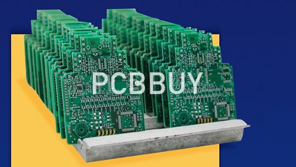
1. Key Advantages of Glass Substrates
Improved dimensional stability and warpage control
Glass can provide high rigidity, good surface flatness, and stable dimensions during fine-pattern fabrication. Its coefficient of thermal expansion (CTE) can also be selected or engineered to help manage thermal expansion mismatch between the substrate and semiconductor dies.
These characteristics are valuable for large chiplet packages, where excessive warpage or layer misregistration can affect fine-pitch interconnections and assembly yield.
Potential for high-speed signal integrity
Glass-core substrates can support low-loss interconnect designs, depending on glass composition, dielectric properties, conductor geometry, and metallization. This makes them promising for high-speed links in AI and HPC packages, where signal loss and routing density can constrain performance.
Nevertheless, glass alone does not guarantee better signal integrity. Copper roughness, via transitions, trace geometry, impedance control, and the complete package architecture must also be considered.
Support for high-density interconnections
Glass substrates can support through-glass vias (TGVs) and fine redistribution-layer (RDL) routing in advanced packaging. These structures can help connect chiplets and other components within compact, high-I/O-density packages.
TGV formation and metallization require specialized processes, however. Glass is brittle, and via formation, copper adhesion, stress management, and reliability validation remain important engineering challenges.
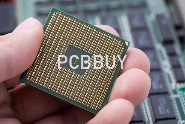
2. Glass Substrates vs Conventional PCB Materials
|
Design consideration |
Glass-core substrate |
Conventional organic PCB substrate |
|
Dimensional stability |
High flatness and dimensional stability can benefit fine-pitch packaging |
Depends on laminate construction, moisture, temperature, and processing |
|
Warpage management |
Glass properties can be engineered to help reduce package warpage |
Warpage can become challenging in large, complex multilayer structures |
|
High-speed electrical performance |
Promising low-loss performance, depending on material and interconnect design |
Low-loss organic laminates are well established for many high-speed applications |
|
Interconnection technology |
Can use TGVs and fine RDL structures in advanced packaging |
Commonly uses plated-through holes, microvias, and HDI structures |
|
Manufacturing maturity |
Specialized processes and qualification are still evolving |
Mature supply chains and established PCB fabrication workflows |
|
Cost and availability |
Depends on process maturity, yield, and package design |
Broad material availability and established manufacturing options |
The right choice depends on the application. Glass-core substrates are particularly relevant to advanced semiconductor packaging, while conventional high-speed PCB materials remain practical for many server motherboards, accelerator cards, networking boards, and power distribution boards.
3. Design and Manufacturing Considerations
Before selecting a glass-core solution, engineers should evaluate the complete package architecture rather than focusing on substrate material alone. Key considerations include:
-
Electrical design: Validate dielectric properties, impedance, insertion loss, crosstalk, and via-transition performance at the target data rates.
-
Thermomechanical reliability: Evaluate CTE compatibility, warpage, thermal cycling, and the reliability of copper-to-glass interfaces.
-
Via and metallization processes: Confirm TGV geometry, copper filling or plating requirements, and inspection methods with a qualified supplier.
-
Manufacturing yield: Consider glass handling, edge damage, via defects, dimensional tolerances, and the availability of suitable process controls.
Glass-core substrate manufacturing should not be confused with conventional PCB fabrication using glass-reinforced epoxy laminate. FR-4 contains woven glass reinforcement within a resin system; a glass-core substrate uses a glass core as a distinct structural platform and may require specialized packaging processes.
4. How PCBBUY Can Support Related High-Speed PCB Projects
Although glass-core semiconductor substrates require specialized manufacturing capabilities, many high-speed computing systems also depend on conventional multilayer PCBs for server backplanes, accelerator cards, networking interfaces, and power delivery.
PCBBUY's published PCB manufacturing capabilities include 1–26-layer boards, selected Rogers high-frequency materials, high-Tg laminates, and HDI options subject to design review. These capabilities may be relevant to conventional PCB portions of high-speed computing systems, but they should not be interpreted as confirmation that PCBBUY manufactures glass-core semiconductor package substrates or TGV structures.
For customers developing computing hardware, PCBBUY can review the PCB-level requirements, including stackup, material selection, impedance targets, copper weight, via structure, and manufacturing tolerances. The appropriate material and process should be confirmed against the actual design rather than selected solely on the basis of a material trend.
The same engineering discipline applies to PCBBUY's target fields, including automotive electronics, industrial control, electrical power, power supplies, energy storage, new energy, and embodied robotics. These applications may use advanced computing and control hardware, but material selection must still reflect each product's electrical, thermal, mechanical, and reliability requirements.
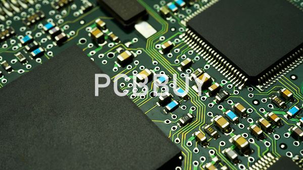
5. Quality Control and Acceptance Requirements
For conventional PCB projects, the fabrication specification should define the approved stackup, laminate grade, finished thickness, copper weight, impedance requirements, and applicable acceptance criteria. Inspection and testing should follow the purchase order, relevant IPC requirements, and customer specifications.
Depending on the board design, PCBBUY's published quality processes include AOI and electrical testing. High-speed projects may also require impedance testing, signal-integrity validation, or additional documentation specified by the customer. These checks should be agreed upon before production.
For glass-core packaging projects, customers should separately confirm the supplier's capabilities for TGV formation, metallization, dimensional control, package-level inspection, and reliability qualification.
Conclusion
Glass substrates offer promising advantages for high-speed computing, especially in dimensional stability, warpage management, fine interconnections, and potential low-loss signal transmission. Their suitability still depends on package design, electrical requirements, manufacturing maturity, and reliability validation.
For conventional high-speed PCBs used alongside AI and HPC packages, PCBBUY offers multilayer fabrication, selected high-frequency materials, and HDI manufacturing options. Early engineering review helps determine the appropriate material system and avoid confusing conventional PCB capabilities with specialized glass-core substrate manufacturing.
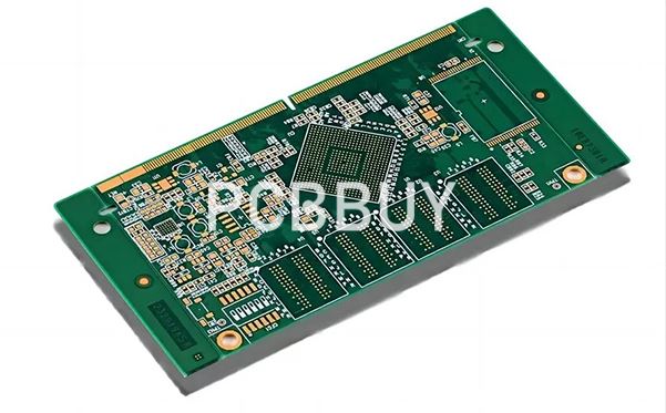
FAQ
1. What are the main advantages of glass substrates for high-speed computing?
Key potential advantages include high flatness, dimensional stability, reduced warpage in suitable designs, support for dense interconnections, and low-loss electrical performance depending on the material and interconnect structure.
2. Are glass substrates better than FR-4 for every high-speed PCB?
No. Glass-core substrates are mainly attracting attention in advanced semiconductor packaging. FR-4 and specialized low-loss organic laminates remain suitable for many high-speed PCBs, depending on signal frequency, loss budget, cost, and manufacturing requirements.
3. What is a through-glass via (TGV)?
A TGV is a conductive interconnection formed through a glass substrate. It can connect conductive layers or redistribution structures in advanced packages. TGV fabrication requires specialized hole formation and metallization processes.
4. Does PCBBUY manufacture glass-core semiconductor substrates?
PCBBUY's published capabilities describe conventional multilayer PCB fabrication, HDI options, and selected high-frequency materials. Glass-core substrate and TGV manufacturing should be confirmed separately; the published PCB capabilities do not establish that these specialized processes are available.
5. What should engineers verify when choosing a substrate for high-speed computing?
Evaluate dielectric properties, insertion loss, impedance, copper roughness, via transitions, dimensional stability, CTE compatibility, thermal behavior, manufacturing yield, and the supplier's verified process capabilities. The decision should be based on the complete electrical and mechanical design.
Industry Category