HDI PCB Layout Capabilities and Manufacturing Expertise
By:PCBBUY 06/23/2025 16:14
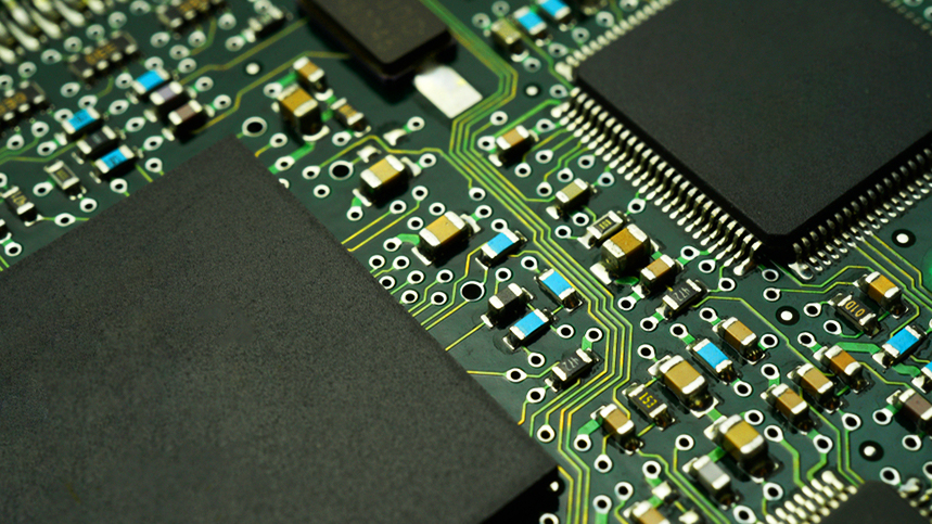
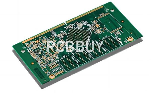
As the demand for high-performance and miniaturized electronics continues to rise, High Density Interconnect (HDI) PCB layout has become the go-to solution for advanced electronic applications. At PCBBUY, we specialize in delivering high-quality HDI PCB layout and fabrication services that meet the exacting demands of global clients.
What is HDI PCB Layout?
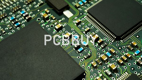
HDI (High Density Interconnect) PCB layout refers to the strategic design of PCBs with higher wiring densities per unit area. This is achieved by utilizing finer lines and spaces, smaller vias, and higher connection pad density, which allows for more functionality in a smaller footprint.
At PCBBUY, our HDI PCB layouts are optimized for signal integrity, electrical performance, and space efficiency, making them ideal for smartphones, tablets, wearable devices, medical electronics, and automotive systems.
HDI PCB Layout Design & Construction Types
One of the cornerstones of HDI PCB layout is the stack-up and via structure. PCBBUY supports both first-order and second-order HDI constructions:
-
1st Order HDI: 1+N+1, 1+1+N+1+1 (n buried vias ≤ 0.3mm)
-
2nd Order HDI: 2+N+2, 1+2+N+2+1 (n buried vias ≤ 0.3mm)
These configurations allow us to offer enhanced electrical routing and reduced signal loss. Based on your design requirements, our engineering team will recommend the most suitable layout using mechanical via or via filling + electroplating technologies.
Core Materials Used in HDI PCB Layout
PCBBUY utilizes top-grade materials to ensure excellent reliability and thermal performance:
-
Base Material: FR-4
-
Optional Materials: TG135-TG170, halogen-free materials, CTI rated laminates (customizable)
Material selection is flexible depending on the project requirements and end-use application, with an emphasis on high thermal stability and flame retardance.

HDI PCB Layering Capabilities
We support a wide range of layer configurations to meet the needs of various industries:
-
Standard HDI Layers: 4–10 layers (1st Order)
-
Advanced HDI Layers: 6–16 layers (2nd Order)
For more complex layouts, our pcb production lines are capable of fabricating high-density multilayer PCBs with precision.
Manufacturing Precision for HDI Layouts
PCBBUY delivers highly accurate PCB manufacturing parameters to ensure high signal integrity and minimal interference:
|
Parameter |
Capability |
Notes |
|
Trace Width |
2/2 mil (minimum) |
Ideal for fine-pitch BGA layout |
|
Blind Via |
≥0.15mm (mechanical), ≥0.075mm (laser) |
Suitable for microvia interconnects |
|
Hole Size |
Minimum 0.3mm unilateral |
High precision CNC drilling |
|
Hole Copper Thickness |
>18um (mechanical), >13um (laser blind burial) |
Fully filled and reliable |
|
Via Electroplating |
Depth 0.05–0.1mm, Tolerance: ±15% |
Ensures complete metal coverage inside vias |
Advanced Via Technology in HDI Layout
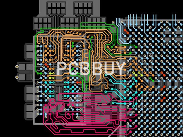
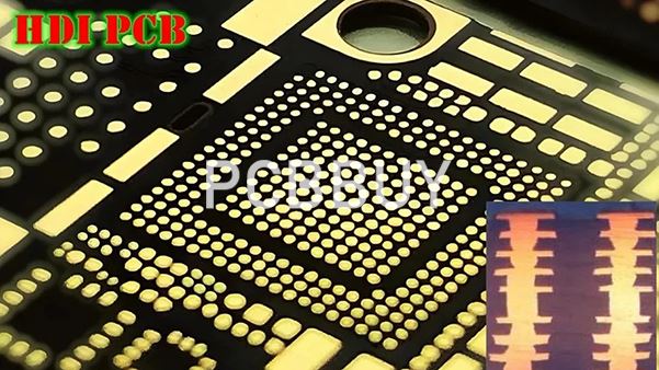
HDI layout often requires a combination of blind vias, buried vias, and microvias. PCBBUY provides both mechanical drilling and laser drilling options depending on the PCB structure. Laser vias are commonly used in HDI stack-ups due to their accuracy and ability to fit within ultra-fine pitch devices.
Our via electroplating process fills the via with copper, ensuring strong conductivity and long-term durability. We also offer stacked and staggered via structures, ideal for 2+N+2 or 3+N+3 layouts.
Why Choose PCBBUY for HDI PCB Layout & Fabrication?
-
Engineering Expertise: Decades of experience in HDI layout and production.
-
End-to-End Service: From stack-up planning to layout optimization to mass production.
-
Customization: Flexible construction types, material options, and layer count.
-
International Quality: IPC Class 2/3 standards, RoHS compliant, UL and ISO certified.
-
Responsive Service: 24-hour engineering support and rapid prototyping.
HDI PCB Layout FAQ
What is the difference between a standard PCB layout and an HDI PCB layout?
Answer:
HDI (High-Density Interconnect) PCBs use advanced technologies such as laser-drilled microvias, blind/buried vias, and ultra-fine trace/spacing to achieve higher component density, smaller board sizes, and better signal performance compared to standard PCB layouts.
Key Comparison Chart:
|
Feature |
Standard PCB |
HDI PCB Layout |
|
Via Types |
Through-hole |
Microvia, Blind/Buried |
|
Min. Trace/Spacing |
≥ 4/4 mil |
≥ 2/2 mil |
|
Board Density |
Medium |
High |
|
Application |
Consumer Electronics |
Mobile, Medical, Auto |
What is the typical layer stack-up for HDI PCB at PCBBUY?
Answer:
PCBBUY supports complex stack-up structures such as:
🔹 1+N+1 (Single-order HDI)
🔹 2+N+2, 3+N+3 (Multi-order HDI)
🔹 Via-in-pad, staggered vias, and copper-filled vias
📐 Example Stack-up:
Top Layer (L1)
│
Blind Via
▼
Core Layer (L2~Ln)
│
Buried Via
▼
Bottom Layer (Ln+1)
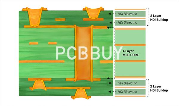
Based on your design, we recommend the optimal stack-up to ensure performance, reliability, and manufacturability.
What are PCBBUY’s capabilities in trace width and spacing for HDI layout?
Answer:
✅ Minimum Trace Width: 2 mil (0.05 mm)
✅ Minimum Spacing: 2 mil (0.05 mm)
Tip: We recommend ≥ 4 mil to reduce cost and improve yield unless ultra-dense routing is required.
Technology Used:
Laser Direct Imaging (LDI)
Automated Etch-Back
AOI Inspection
How are blind and buried vias implemented at PCBBUY?
Answer:
We use:
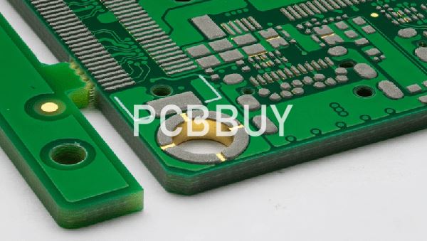
Laser drilling for blind vias (≥0.075 mm)
Mechanical drilling for buried vias (≥0.15 mm)
Electroplated via filling for strength and conductivity
±15% tolerance control for consistent depth
Via Process Options:
|
Via Type |
Tech Used |
Min. Size |
Application |
|
Blind |
Laser Drill |
0.075 mm |
L1 → L2 or Ln → Ln-1 |
|
Buried |
Mechanical Drill |
0.15 mm |
L2 → L3 (internal layers) |
|
Microvia |
Laser Drill + Fill |
0.1 mm |
HDI density builds |
Can PCBBUY support customized materials for HDI PCB layout?
Answer:
Absolutely. While FR-4 is the standard base material, we also offer:
✅ TG135–TG170 High-Tg
✅ Halogen-Free Laminates
✅ CTI Customized Substrates
These are ideal for high-frequency, thermal, or environmental compliance requirements.
What applications are HDI PCBs most suitable for?
Answer:
HDI PCBs are essential in industries requiring high performance and compact size, such as:
Aerospace & Defense
Smartphones & Wearables
Automotive Radar & EV Systems
High-Speed Computing & Servers
Medical Imaging Devices
How does PCBBUY ensure the quality of your HDI PCB layout?
Answer:
PCBBUY follows a rigorous QC process, including:
Automated Optical Inspection (AOI)
Laser depth profiling for vias
Impedance Control Simulation
X-ray via inspection
IPC Class 2 & 3 Standards
We are ISO 9001, RoHS, and UL certified to meet global quality requirements.
Start Your HDI PCB Layout Project with PCBBUY
PCBBUY is committed to providing innovative and reliable HDI PCB layout services to customers worldwide. Whether you are in the prototyping phase or need large-volume production, our technical team is ready to assist you from start to finish.
Contact us today to upload your design files and receive a free HDI layout consultation.
Industry Category


