Heavy Copper PCB Quality Inspection: What to Check Beyond Electrical Testing
By:PCBBUY 11/11/2026 17:22
Introduction
A heavy copper PCB can pass a flying probe electrical test and still develop reliability problems in a high-current, high-temperature application. Electrical testing answers an important question—whether the required circuits are electrically connected and isolated at the time of testing—but it does not reveal every potential manufacturing defect.
For example, an electrical test may not show whether plated copper is thinner at the center of a high-aspect-ratio hole, whether excessive etching has reduced conductor spacing, or whether resin has adequately filled critical areas around thick copper features.
For heavy copper PCB quality inspection, a more complete approach combines visual inspection, dimensional measurement, cross-section analysis, and thermal stress testing. These inspection methods address different failure modes and should not be treated as interchangeable.
For heavy copper PCB applications in automotive electronics, industrial control, power supplies, energy storage, new energy systems, and advanced robotics, PCBBUY applies inspection planning based on the structure and reliability requirements of the product.

1. Heavy Copper PCB Inspection Does Not Mean Every Test Is Performed on Every Board
One common misunderstanding is to interpret “100% inspection” as requiring every quality test to be performed on every finished PCB. In practice, inspection methods have different frequencies because some tests are non-destructive while others require destructive sampling.
A practical inspection structure can be divided into three levels:
|
Inspection level |
Typical items |
Inspection approach |
|
100% non-destructive inspection |
Appearance, key dimensions, hole features, electrical continuity and isolation |
Individual production boards |
|
Batch or process verification |
Cross-section analysis, plating structure, resin filling and annular ring evaluation |
Coupons, first articles, or qualified samples |
|
Reliability verification |
Thermal stress testing followed by structural evaluation where required |
Test specimens or representative samples |
Microsection analysis is destructive, so it is generally performed on test coupons or representative samples rather than every finished PCB. For heavy copper boards, the critical issue is not simply increasing the number of cross-sections. It is selecting inspection locations that can reveal the most relevant manufacturing risks.
Likewise, thermal stress testing is typically used as a reliability or batch verification method. Its value increases significantly when the tested structure is evaluated after thermal exposure rather than relying only on visible changes.
2. Visual Inspection: What Should Be Checked on a Heavy Copper PCB?
Visual inspection remains the first screening layer, but heavy copper boards require attention to manufacturing effects associated with thicker copper.
Conductor Edges and Etching
Thicker copper generally creates a more challenging etching process. Side etching can affect the final conductor profile, particularly in fine-line areas.
PCBBUY's process capability data shows that thicker copper designs require different line-width and spacing considerations than standard thin-copper boards. During inspection, engineers should pay attention to:
-
Excessive undercut at conductor edges.
-
Localized conductor narrowing.
-
Uneven copper distribution after plating and etching.
-
Areas where reduced spacing could affect electrical isolation.
A trace can still pass an electrical continuity test even if localized geometry changes create higher current density or reduced reliability margins.
Via and Hole Openings
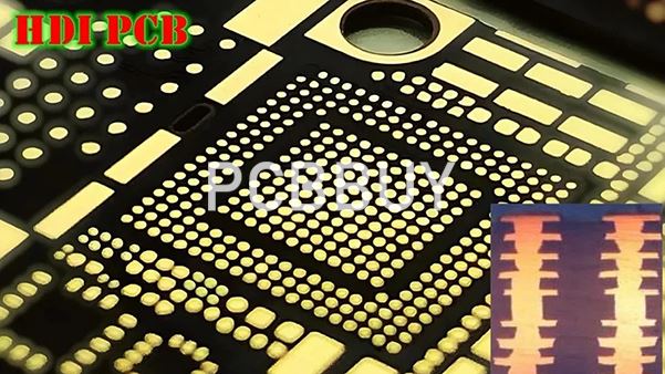
Hole openings deserve particular attention because they can become localized stress areas. Depending on the design and process, some visible conditions around a via opening may be process-related, while plating separation or obvious ring-shaped defects require further investigation.
Visual inspection should therefore focus on the integrity of the connection between the plated hole structure and surrounding copper.
Solder Mask Around Thick Copper Features
Thick copper creates larger surface steps, which can make solder mask coverage more difficult to control. The coating thickness near copper edges may differ from the thickness on flat areas.
Inspectors should look for:
-
Incomplete solder mask coverage near copper edges.
-
Signs of copper exposure.
-
Registration issues.
-
Inconsistent filling or coverage around plugged holes.
Visual inspection cannot replace cross-section analysis or reliability testing, but it is an efficient screening method. Areas showing abnormal visual characteristics may also require additional investigation during engineering review.
3. Dimensional Inspection: Copper Thickness Changes the Manufacturing Picture
Heavy copper PCB dimensional inspection involves more than checking the board outline or finished hole diameter.
Finished Copper Thickness
Copper thickness should be evaluated according to the finished board requirements. PCBBUY's published manufacturing standards include finished outer-layer copper acceptance values of:
-
1 oz: ≥35 μm
-
2 oz: ≥70 μm
-
3 oz: ≥105 μm
These values should be interpreted together with the PCB construction and customer requirements. Inner-layer copper values may differ from finished outer-layer copper because of the material and manufacturing process.
For this reason, specifying only “3 oz copper” does not provide a complete quality requirement. Engineering documentation should clearly identify the required finished copper construction and the applicable acceptance criteria.
Trace Width and Spacing Distribution
Heavy copper etching can affect final trace geometry. Measuring only one location may not show how the manufacturing process varies across the panel.
For critical designs, dimensional evaluation should consider representative locations, such as:
-
Central board areas.
-
Edge areas.
-
Isolated or high-current copper features.
This helps engineers evaluate whether etching and plating variations remain within the intended design margins.
Hole-to-Copper Clearance
Drilling and routing accuracy are important, but finished dimensions should also be evaluated in relation to surrounding copper.
For high-voltage or high-power applications, insufficient clearance between holes, copper features, and board edges can affect insulation and creepage performance. This is particularly important in power electronics and energy storage products.

4. Cross-Section Analysis: The Most Valuable Internal Inspection Method
Cross-section analysis provides information that visual inspection and electrical testing cannot show directly.
A properly prepared microsection can help evaluate:
-
Plated-through-hole copper distribution.
-
Minimum copper thickness.
-
Layer registration.
-
Annular ring condition.
-
Internal plating defects.
-
Resin filling and dielectric structure.
Evaluate the Minimum Copper Condition, Not Only the Average
In high-aspect-ratio holes, plating distribution may vary between the hole entrance and the center. The center of the hole can be one of the most critical locations for evaluating copper coverage.
For this reason, a cross-section report should provide meaningful measurement information rather than relying only on a single average value.
PCBBUY offers different plated-hole copper options, including 18 μm, 20 μm, 25 μm, 30 μm, and 35 μm grades. The appropriate requirement should be selected according to the board structure, application environment, and customer specification.
Select Cross-Section Locations Based on Risk
A single cross-section location cannot represent every manufacturing condition on a heavy copper PCB.
A practical inspection strategy may include different locations for different purposes:
-
Board center: useful for evaluating plated-hole copper and internal layer structure.
-
Board edge: useful for reviewing conductor geometry and process variation.
-
Critical structural areas: selected based on thick copper features, annular rings, resin flow, or other design-specific risks.
Test coupons can provide routine process monitoring, while first-article or representative samples may be used for additional structural verification when required.
Distinguish Different Types of Voids
Not every internal void has the same cause or reliability implication. Plating-related voids and resin-filling voids should be evaluated according to the applicable product requirements and inspection criteria.
A useful cross-section report should therefore describe the defect type and inspection location rather than simply stating that the board “passed cross-section inspection.”

5. Thermal Stress Testing: The Test Temperature Is Only Part of the Inspection
Thermal stress testing is particularly relevant to heavy copper PCBs because thick copper structures and dielectric materials respond differently to temperature changes.
Copper and PCB dielectric materials have different coefficients of thermal expansion. During thermal exposure, these differences can create mechanical stress at plated holes, copper corners, and layer interfaces.
PCBBUY's published reliability requirements include a thermal shock condition of 288±5°C for 10 seconds, repeated three times for applicable products.
However, the value of thermal stress testing does not come only from the test condition itself. Engineers also need to consider what is evaluated after the thermal exposure.
Potential post-test concerns may include:
-
Cracking in plated-hole structures.
-
Separation at copper-to-dielectric interfaces.
-
Delamination.
-
Structural changes around critical copper features.
For this reason, thermal stress testing and post-test structural evaluation can form a stronger verification process than visual inspection alone. Where required by the product specification, cross-section analysis after thermal testing can help identify defects that are not immediately visible or electrically detectable.
For products exposed to frequent temperature cycling, such as automotive electronics, energy storage equipment, and motor or robotic drive systems, additional application-specific reliability testing may also be required.
A Practical Heavy Copper PCB Inspection Workflow
|
Inspection stage |
Main focus |
Defects or risks addressed |
|
Visual inspection |
Copper edges, hole openings, solder mask coverage |
Undercut, exposed copper, coating defects |
|
Dimensional inspection |
Copper thickness, trace geometry, holes and clearances |
Geometry variation and reduced design margins |
|
Cross-section analysis |
Plating, internal structure, resin filling |
Internal defects not visible during electrical testing |
|
Thermal stress verification |
Structural performance after thermal exposure |
Cracking, interface separation and thermal weakness |
The most effective inspection process is not simply a longer checklist. Each stage should provide information that the previous stage cannot.

FAQ
Q1: If a heavy copper PCB passes electrical testing, why are cross-section analysis and thermal stress testing still needed?
Electrical testing verifies electrical continuity and isolation under the specified test conditions. It does not directly show the internal geometry or material condition of a plated hole.
A board may remain electrically functional even when a copper area is close to its minimum thickness requirement or when a latent structural defect has not yet developed into a complete open circuit.
Cross-section analysis helps evaluate the internal manufacturing structure, while thermal stress testing can reveal how critical interfaces respond to elevated temperature. These methods provide different information and should not be considered replacements for one another.
Q2: Is 100% cross-section inspection realistic for heavy copper PCBs?
Cross-section analysis is destructive, so cutting every finished PCB is generally not practical.
A more effective approach is to define an inspection plan using coupons, first articles, representative samples, and additional verification points when the material, copper thickness, or board structure changes.
For procurement and engineering review, the key question is not simply how many cross-sections are performed. It is whether the sampling locations and inspection criteria address the actual risks of the heavy copper structure.
Q3: Is 288°C for 10 seconds and three cycles enough for heavy copper PCB verification?
A thermal condition of 288±5°C for 10 seconds, repeated three times can be used as a defined thermal stress verification condition. However, whether it is sufficient depends on the final application and customer requirements.
Products used in demanding environments may require additional qualification testing, such as extended temperature cycling or other application-specific reliability evaluations.
For production inspection, the test plan should distinguish between routine batch verification and broader product reliability qualification.
Q4: What should I ask a PCB supplier about heavy copper inspection capability?
Instead of comparing suppliers based only on a single copper thickness or hole copper value, ask about the complete inspection process.
Useful questions include:
-
What finished copper thickness acceptance criteria are used?
-
How are critical trace width and spacing features verified?
-
What plated-hole copper options are available?
-
How are cross-section locations selected?
-
Can thermal stress verification be combined with post-test structural analysis?
-
What inspection records can be provided for the order?
For heavy copper PCB projects involving automotive, industrial control, power supply, energy storage, new energy, and advanced robotics applications, PCBBUY can support engineering communication on manufacturing requirements and inspection planning.
Conclusion
Heavy copper PCB quality control should not be based on electrical testing alone. A reliable inspection strategy combines different methods because each one identifies different types of manufacturing risk.
Visual inspection provides an efficient first screening layer for conductor edges, hole openings, and solder mask coverage. Dimensional inspection verifies the finished geometry and copper-related design margins. Cross-section analysis reveals internal plating and structural conditions that cannot be seen from the board surface. Thermal stress testing evaluates how critical structures respond to elevated temperature, with post-test structural inspection providing additional evidence when required.
For engineers, this inspection framework helps align copper thickness, trace geometry, plated-hole requirements, and acceptance criteria during design and manufacturing review. For procurement teams, it provides a better way to evaluate whether a supplier has a complete quality verification process rather than relying on a single specification such as “3 oz copper” or one plated-hole thickness value.
PCBBUY supports heavy copper PCB manufacturing for applications where current capacity, thermal performance, and long-term reliability require careful engineering and quality control. By defining inspection requirements early in the project, manufacturers and customers can build a clearer verification path from fabrication to final delivery.
Industry Category