High-Frequency PCB Prototyping: What's the Difference Between a Manufacturer That Can Make It and One That Can Make It Well?
By:PCBBUY 11/19/2026 16:31
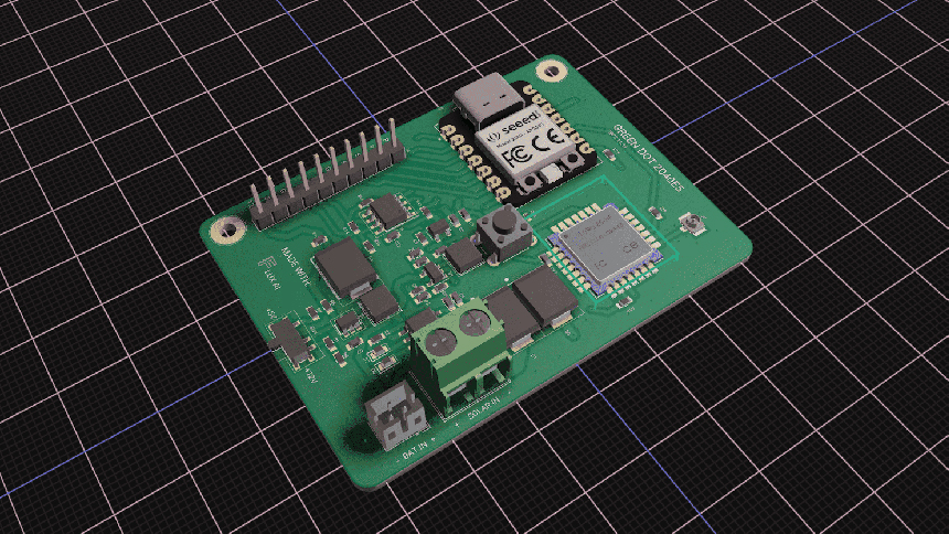
There is one easily overlooked fact about high-frequency PCB prototyping: even when two manufacturers receive the same Gerber files specifying Rogers 4350B material, 50 Ω ±10% impedance, and an immersion gold surface finish, the resulting boards can differ significantly in signal integrity, long-term reliability, and batch-to-batch consistency. The issue is not necessarily that one manufacturer cannot fabricate the board. Rather, the quality of a high-frequency PCB is not determined by a single manufacturing process. It depends on a combination of material expertise, stackup engineering, impedance verification, copper thickness control, and outgoing quality data.
For engineers and procurement teams working in automotive electronics, industrial control, power electronics, energy storage, new energy systems, and embodied robotics, this distinction is particularly important. These applications rarely operate under the assumption that passing a laboratory test is sufficient. The boards must withstand continuous operation, thermal cycling, vibration, and high-voltage pulses over extended periods. High-frequency performance degradation is often gradual and systematic. By the time an issue appears in the end product, the cost saved during prototyping may already have been multiplied several times over.
From a practical engineering perspective, this article examines the questions worth asking when selecting a high-frequency PCB prototyping manufacturer. It also uses Lieban's published manufacturing capabilities and outgoing quality standards as practical reference points.
1. Understand the Difference Between High-Frequency and High-Speed PCBs Before Choosing a Manufacturer
Many RFQs use the term "high-frequency and high-speed PCB" as if the two were interchangeable. However, they refer to different engineering challenges and failure mechanisms.
High-frequency PCBs are typically used to process analog RF signals. Their primary concerns are dielectric loss and phase stability, making the dissipation factor (Df) a critical material parameter. High-speed PCBs, on the other hand, handle digital signals with fast edge rates. Their primary challenges involve impedance continuity and timing alignment.
Confusing these two requirements can lead to two costly mistakes. One is using expensive high-frequency laminate for digital signal paths that could be adequately supported by high-speed FR-4, unnecessarily increasing the BOM cost. The other is using conventional PCB materials in millimeter-wave RF paths, where excessive signal loss and phase drift may not become apparent during initial testing but can develop into systematic problems in mass production.
Therefore, the first step in selecting a manufacturer is not simply asking, "Can you manufacture high-frequency PCBs?" Instead, clearly define the type of signals involved. Are you working with RF or microwave channels above 300 MHz, high-speed digital interfaces such as PCIe, DDR, and Ethernet, or a design that combines both on the same board?
A manufacturer's ability to distinguish between these requirements and recommend an appropriate stackup is far more valuable than a starting price listed for high-frequency PCBs.
In its published technical information, Lieban uses this distinction as the starting point for material selection. Its high-frequency material portfolio covers Rogers, TUC, and Isola product families, while Kingboard and Shengyi FR-4 materials remain available for non-critical layers. The underlying approach is to determine which layers actually require high-frequency performance during the engineering review, rather than attempting to correct material-related problems after fabrication.

2. Material Expertise: Having Rogers Laminate in Stock Does Not Mean Knowing How to Process It
The differences between Rogers, PTFE, ceramic-filled hydrocarbon laminates, and conventional FR-4 extend well beyond their dielectric constant (Dk) and dissipation factor (Df).
PTFE has a highly inert surface, so its drilling parameters, electroless copper activation, and lamination process window differ from those used for FR-4. Ceramic-filled materials also have different brittleness and thermal expansion characteristics, requiring their own process parameters.
A manufacturer that can simply purchase Rogers laminate but has not established dedicated drilling, etching, and lamination controls for that material may produce boards that look normal during prototyping. However, via-wall roughness, interlayer bond strength, and impedance consistency may already be close to their specification limits.
When evaluating a manufacturer, ask whether it maintains separate process parameter libraries for different material systems rather than applying one set of FR-4 parameters to every board.
Lieban's published material capabilities cover FR-4 from Kingboard and Shengyi, halogen-free materials, black-core laminates, Rogers high-frequency materials, TUC materials, and Isola materials. It also supports yellow-core and white-core materials, ultra-high-Tg materials up to Tg 260, and customized high-frequency and high-speed laminates.
Hybrid constructions combining high-frequency materials with FR-4 are also available. This means the manufacturer has predefined process approaches for managing the lamination risks associated with dissimilar material interfaces, rather than treating hybrid lamination as an ordinary multilayer PCB process.
3. Hybrid Stackups: The Lamination Process Window Is the Real Challenge Behind Cost Optimization
A PCB fabricated entirely from high-frequency laminate offers the most straightforward material configuration from an electrical performance perspective, but it also comes with the highest material cost.
Many actual projects use hybrid stackups instead, placing high-frequency materials on critical signal layers while retaining FR-4 for power and ground layers. This approach balances signal integrity requirements with overall BOM cost.
The challenge is that high-frequency laminates and FR-4 can have significantly different coefficients of thermal expansion (CTE). If the temperature profile is not properly controlled during lamination, delamination and warpage may only become apparent during subsequent reflow soldering or long-term thermal cycling.
Hybrid lamination capability should not be judged simply by whether a manufacturer can press the materials together. The more important question is whether the manufacturer evaluates the number of lamination cycles, prepreg selection, and heating and cooling rates during the engineering review.
A widely recognized industry consideration is that when a core undergoes more than a certain number of lamination cycles, typically three or more, a dedicated process review is necessary. For hybrid constructions, the manufacturer should provide lamination parameters and microsection data during prototyping rather than simply delivering a board that shows no visible signs of delamination.
Lieban's customized manufacturing capabilities include custom lamination structures, asymmetric hybrid lamination, and hybrid constructions using dissimilar materials. These capabilities are intended to address designs in which high-frequency laminates and FR-4 coexist.
Its double-prepreg and multiple-prepreg designs are used in heavy copper and high-frequency hybrid applications to improve dielectric strength and resistance to high-voltage breakdown. The purpose is not simply to reduce costs by using a single prepreg layer.

4. Impedance: Calculation, Control, Measurement, and Reporting Are Four Different Things
Asking a manufacturer, "Can you control impedance?" is too broad a question to provide meaningful engineering information.
From an engineering perspective, impedance matching involves theoretical simulation and calculation based on the customer's design. Impedance control refers to managing manufacturing parameters to keep actual impedance values within the specified range. Impedance testing involves instrument-based verification during first-article inspection, in-process inspection, and final inspection. An impedance report records the test results as traceable quality data.
In many cases, what manufacturers advertise as "free impedance control" only covers the first step: running a calculation in engineering software, using a default stackup, and releasing the board for fabrication without impedance coupons or TDR measurements.
For automotive, industrial control, energy storage, and robotics applications involving continuous operation and thermal cycling, the risk of skipping these steps is not that failure is inevitable. It is that a problem may remain undetected until the board is integrated into the end product, when identifying its root cause becomes much more difficult.
Three parameters deserve particular attention during high-frequency PCB prototyping: impedance tolerance, measurement method, and dielectric thickness control.
The typical industry impedance tolerance is ±10%, while more demanding projects often require tolerances within ±5%.
Lieban's published narrow-tolerance impedance control capability is generally within ±5%, with tighter tolerances available for certain high-requirement projects. Its engineering team uses tools such as Polar SI9000 for stackup and impedance calculations. LDI exposure helps maintain tighter trace-width tolerances, while TDR measurements are used for verification throughout the process.
Its outgoing quality specifications include the following parameters:
| Parameter | Kingboard / Guoji | Kingboard / Shengyi |
|---|---|---|
| Registration Accuracy | ±4 mil | ±3 mil |
| Average Plated Copper Thickness | 18–20 μm | 20–25 μm |
| Available Acceptance Standard | IPC-A-600J Class 2 or Class 3 | IPC-A-600J Class 2 or Class 3 |
Procurement teams and engineers can use these figures to compare the manufacturer's capabilities with their project requirements instead of relying on a general statement that the supplier offers impedance control.
Another easily overlooked detail is whether the impedance coupon is fabricated using the same panel, lamination cycle, and etching process as the actual PCB. Even if a separately fabricated test coupon passes impedance testing, its results may not fully represent the impedance of the actual traces on the board.
Lieban fabricates impedance coupons alongside the production boards using the same manufacturing process. First-article, in-process, and final impedance inspections are performed using Weichuangxing impedance testing equipment.
Its stated measurement ranges cover single-ended impedance from 10–150 Ω and differential impedance from 20–200 Ω, with a measurement accuracy of ±1% and a minimum resolution of 0.01 Ω.
5. Via Copper and Copper Thickness: High-Frequency PCBs Require More Than Surface Trace Inspection
The skin depth of a conductor decreases rapidly as frequency increases. At 77 GHz, the skin depth of copper is approximately 0.24 μm, while the surface roughness of standard electrodeposited copper foil can reach 4–8 μm.
As a result, the actual current path can be considerably longer than the ideal geometric path, significantly increasing conductor loss.
This means copper foil roughness and copper thickness uniformity directly affect impedance and insertion loss in high-frequency PCBs. They should not be evaluated using the same simple "copper thickness meets specification" approach commonly applied to conventional PCBs.
For plated copper thickness in through-holes, the default average value under IPC Class 2 is 18 μm. However, a common industry practice is to accept individual measurement points around 16 μm, even when the average value meets the nominal requirement.
For automotive electronics, industrial control, power and energy storage, and embodied robotics, where electrical connection stability is particularly important, it is more meaningful for a manufacturer to offer higher default copper thickness targets and multiple selectable levels, such as 20 μm, 25 μm, 30 μm, and 35 μm, rather than simply labeling its capability as "18 μm."
Lieban's outgoing quality specifications list the following values:
| Parameter | Kingboard / Shengyi | Kingboard / Guoji |
|---|---|---|
| Average Plated Copper Thickness | 20–25 μm | 18–20 μm |
| Copper Ductility | ≥20% | ≥15% |
For finished surface copper thickness, its stated capabilities include:
| Copper Thickness | Minimum Finished Surface Copper Thickness |
|---|---|
| 1 oz | ≥35 μm |
| 2 oz | ≥70 μm |
| 3 oz | ≥105 μm |
Higher copper thicknesses can also be specified, with heavy copper capabilities extending up to 15 oz. Localized heavy copper can be used in designs that combine high-current requirements with high-frequency impedance control.
The value of these specifications is not that thicker copper is always better. It is that the manufacturer offers graded copper thickness options for different application requirements instead of applying a single default value to every project.
6. Inspection and Outgoing Reports: The Last Thing to Cut During Prototyping
The deliverables for a high-frequency PCB prototype should not consist of just the bare boards and a shipping document.
Passing a continuity test during prototyping does not prove that the board's impedance distribution, plated copper thickness, interlayer registration, or material Dk consistency has been verified.
Microsection reports, impedance test data, and TDR waveforms generated during prototyping establish a baseline for subsequent mass-production transfer and failure analysis. If the manufacturer does not retain these records during the prototype stage, engineers will have no traceable reference when batch-to-batch variations appear during mass production.
Lieban's inspection equipment includes X-ray systems for checking registration in high-layer-count laminations and drilled-hole alignment, metallographic microscopes for analyzing via walls and plating microstructures, CMI600 and CMI165 instruments for measuring plated hole copper and surface copper thickness, and four-wire low-resistance flying probe testing for identifying functional risks such as insufficient via copper, circuit defects, and localized copper-thickness variations.
For outgoing documentation, Lieban can provide outgoing inspection reports, test reports, and impedance reports with impedance coupons for Kingboard / Shengyi material combinations, depending on the product design.
For automotive and industrial control customers, this means the prototype can enter the next development stage with a verifiable data package rather than relying solely on the supplier's assurance that the board is acceptable.
FAQ
Q1: Is choosing Rogers laminate enough when ordering a high-frequency PCB prototype?
No. Rogers is a material brand, not a guarantee of manufacturing quality.
Even when the same RO4350B laminate is used, differences in drilling parameters, lamination profiles, and etching compensation between manufacturers can lead to significant variations in via-wall quality, dielectric thickness consistency, and actual impedance values.
Lieban addresses this by linking material selection with stackup engineering review. The process begins by identifying which signal layers require high-frequency materials and which can retain FR-4. The corresponding drilling and lamination parameters are then selected according to the material system, rather than processing every Rogers board using the same manufacturing workflow.
Q2: If a manufacturer says it has fabricated hybrid laminates before, does that mean its process is reliable?
Being able to laminate dissimilar materials and being able to do so consistently are two different things.
The reliability of a hybrid stackup depends on CTE compatibility, prepreg selection, and control of heating and cooling rates. It is not simply a matter of whether the lamination press can reach the required temperature.
Lieban supports asymmetric hybrid lamination and hybrid structures using dissimilar materials. It also evaluates the lamination structure as a separate customization requirement. At high-frequency material and FR-4 interfaces, the process team focuses on dielectric layer uniformity and interlayer bond strength rather than directly applying the lamination window used for conventional multilayer PCBs.
Q3: What is the difference between free and paid impedance services for high-frequency PCB prototyping?
The difference lies in the depth of verification.
A free impedance service that only performs theoretical calculations, without fabricating impedance coupons or conducting TDR measurements, essentially completes only the impedance-matching stage. It does not provide the full impedance-control and testing process.
Lieban's process starts with theoretical calculations, followed by the fabrication of impedance coupons alongside the actual PCB. An impedance testing instrument is then used for first-article, in-process, and final inspections. An impedance report can also be provided when required.
For applications such as energy storage BMS, robotic joint drives, and automotive radar, where impedance drift can affect system performance, obtaining actual measurement data during prototyping is more valuable in the long term than saving the cost of impedance testing.
Q4: High-frequency PCBs and heavy copper PCBs appear to have conflicting requirements. Can both be combined on the same board?
Yes, but it is important to distinguish between full-board heavy copper and localized heavy copper.
Using heavy copper across the entire board can limit fine-line fabrication capability and increase manufacturing costs. Localized heavy copper, on the other hand, increases copper thickness only in areas that need to carry high current, while maintaining high-frequency materials and fine traces in signal regions.
Lieban supports heavy copper fabrication up to 15 oz, including localized heavy copper structures. For high-power applications such as energy storage systems and new energy vehicles, this zoned approach is more practical than increasing copper thickness across the entire board.
Q5: Should I request microsection and impedance reports during prototyping? Will this increase the cost?
For projects involving automotive electronics, industrial control, power and energy storage, and embodied robotics, requesting these reports is recommended.
Microsection and impedance data generated during prototyping establish a baseline for subsequent mass-production transfer. Without this baseline, when insufficient via copper or impedance drift appears during mass production, engineers may struggle to determine whether the cause is related to the design, material batch variation, or manufacturing process drift.
Lieban's outgoing quality specifications include test reports and impedance reports as available deliverables for Kingboard / Shengyi material combinations. Its inspection equipment also covers plated copper thickness, surface copper thickness, X-ray interlayer inspection, and metallographic microsection analysis. This provides a practical basis for retaining and reviewing prototype quality data.
Conclusion
Choosing a high-frequency PCB prototyping manufacturer is fundamentally about selecting an engineering partner capable of connecting material selection, stackup design, impedance control, copper thickness management, and inspection into a traceable manufacturing process. It is not simply about finding a factory that drills boards according to Gerber files and quotes a price per square meter.
For projects in automotive electronics, industrial control, power electronics, energy storage, new energy systems, and embodied robotics, high-frequency performance is only one part of overall product reliability. Continuous operation, thermal cycling, high-voltage pulses, and vibration can turn every verification step skipped during prototyping into a potential risk in the end product.
Lieban's capabilities across this manufacturing chain are clearly defined: its high-frequency material portfolio covers Rogers, TUC, and Isola, with hybrid lamination support; its impedance process extends from theoretical calculation to TDR measurement; plated copper and surface copper thickness are available in different grades according to application requirements rather than a single default specification; and its inspection equipment and outgoing reports support prototype data retention.
Whether these capabilities are suitable for a specific project still depends on its stackup structure, signal type, and reliability requirements. However, they provide concrete engineering points that customers can ask about and verify, rather than relying on a general statement that the manufacturer can handle high-frequency PCBs.
Industry Category