How to test solder joints?
By:PCBBUY 08/03/2021 17:22

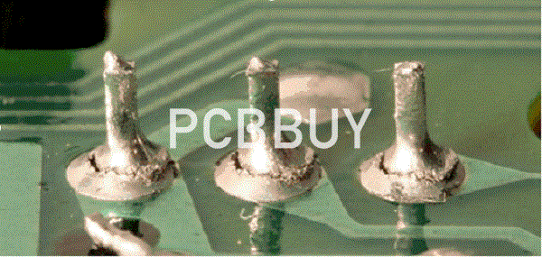
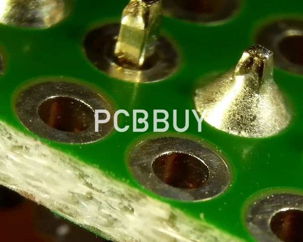
When it comes to optimal BGA assembly achievement, BGA solder joints play an essential role in contributing to the final quality of BGA assembly. Therefore, this article will discuss some effective measures for quality control on BGA solder joints. In this passage, we are talking about the measures for controlling the BGA solder joints in PCB manufacturing. Come and check the content below for more professional knowledge.
What are the common issues of BGA solder joints inspection?
Up to now, as far as manufacturers involved in electronics assembly concerned with BGA components used at a medium or large scale, soldering defects of BGA components are exposed through the implementation of electrical tests. Other methods to control assembly process quality and identify defects on BGA solder joints include sample test on paste screening, X-ray inspection and electrical test analysis.
It's an extremely challenging task to meet assessment requirement for electrical test on BGA components since it's quite difficult to pick up test points under BGA components. Thus, electrical tests can never be relied on BGA defects inspection and assessment, which increases the cost of defect removal and rework to some extent. Electrical tests can only judge whether current is on or off when BGA components get connected. With non-physical solder joint test assisted, it'll be beneficial for assembly process improvement and SPC (Statistical Process Control).
BGA SMT assembly is just a fundamentally physical connecting technology. To be able to determine and control the quality of such a type of process, physical elements should be known and inspected affecting its reliability on long-term operation such as solder paste amount, alignment between leads and pad and wettability.
What are the defects of BGA solder joints?
Open Circuit in Non-collapsible BGA Solder Joints
Open circuits at non-collapsible BGA solder joints usually result from pad pollution. Because solder fails to get pad on PCB wetted, it'll climb onto solder balls and then on component surface. As is discussed in previous part, electrical test can determine the existence of open circuits but fails to determine the real cause of defects.

With cross-section X-ray inspection technology applied, image slices obtained between pad and component layer can be used to distinguish open circuits occurring as a result of pollution. Open circuits as a result of pollution tend to generate small pad radius and large component radius, distinctions between component radius and pad radius can be used to determine whether open circuits take place as a result of pollution. If open circuits take place due to insufficient solder, difference between component radius and pad radius will be very small and this type of difference can be only indicated by cross-section X-ray inspection devices.
Voiding in Collapsible BGA Solder Joints
Voiding in collapsible BGA solder joints takes place because flowing steam is stopped at solder connections with low eutectic point, which is a leading defect held by collapsible BGA components. During the process of reflow soldering, since the influence of floatage generated by voiding concentrates at component surface, majority of solder joint failures take place there as well.
Voiding can be eliminated through preheating during reflow soldering process and short preheating time adding and relatively low preheating temperature. If voiding goes beyond regulated size, number or density, the reliability of components will be dramatically reduced. Voiding in collapsible BGA components can be clearly indicated by cross-section X-ray image slice. Some voiding can be determined and measured within those images or indirectly indicated by the obvious image at BGA solder joints.
How to fix solder joints with BGA inspection?
It's of essential significance to test physical features of BGA solder joints and determine the method of reliable connection achievement during assembly process because the feedback provided by the test is associated with adjustment of each process or calls for parameter adjustment of solder joints.
Physical tests are capable of demonstrating changes of paste screening and everything concerning BGA solder joints during the whole reflow soldering process. Moreover, they are also capable of indicating all the situations concerning all BGA components mounted on a PCB (printed circuit board) or across different PCBs. For example, during the process of reflow soldering, the change of extreme environment humidity along with cooling time will be quickly reflected through BGA voiding count and size. After BGA components are well manufactured, assembly process still needs numerous tests but with inspection depth reduced.
Up to now, X-ray inspection devices applied by lots of manufacturers for electrical test result analysis also holds issues of their incapability to test the reflow soldreability of BGA soldering joints. With an X-ray inspection device applied, the image of solder printed on pad indicates as "shadow" since solder is above solder joint. When it comes to non-collapsible BGA components, shadow also takes place due to front-positioned solder balls.
An X-ray inspection device with only cross-section X-ray inspection technology is capable of breaking the limitation mentioned above because cross-section X-ray inspection devices can get hidden defects exposed of solder joints and can demonstrate BGA soldering connections through the focus on solder joints on pad layer.
When it comes to solder volume and its distribution at solder joints, cross-section images or horizontal slices are applied for measurement. Together with multiple slice measurement of same-type BGA solder joints, 3D test can be effectively provided.
Industry Category


