Inside a Professional HDI PCB Factory
By:PCBBUY 06/30/2025 15:44
In the ever-evolving world of electronics, High-Density Interconnect (HDI) PCBs have become a fundamental component in compact, high-performance devices. As a global HDI PCB factory with over 10 years of industry experience, PCBBUY delivers advanced manufacturing processes, strict quality control, and tailored engineering support to clients across automotive, medical, aerospace, and consumer electronics sectors. This article explores what makes a world-class HDI PCB factory and showcases the high-end capabilities offered by PCBBUY.
HDI PCB Factory Infrastructure
Cleanroom Environments for Precision
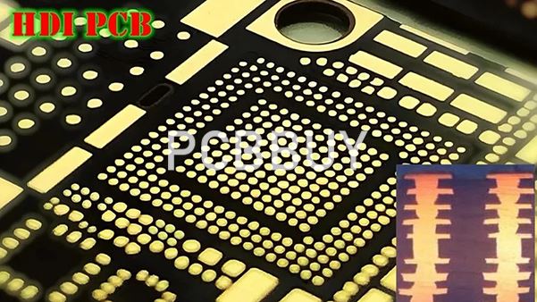
In an HDI PCB factory like PCBBUY, environmental control is paramount. We operate Class 1000–10000 cleanroom facilities to minimize contamination during laser via drilling and imaging processes. This ensures trace precision and via cleanliness necessary for HDI stack-ups with microvias and ultra-thin traces.
Advanced Equipment for High-Resolution Manufacturing
PCBBUY is equipped with industry-leading production lines, including:
-
Laser Direct Imaging (LDI) for sub-50μm resolution
-
CO2 and UV laser drilling machines supporting via sizes down to 0.075mm
-
Vacuum lamination press systems for stable multilayer alignment
-
Automated Optical Inspection (AOI) and Flying Probe Testers for real-time defect detection
-
Automated plating lines for uniform copper filling and high aspect ratio via integrity
Comprehensive HDI PCB Factory Capabilities at PCBBUY
HDI Layer Stackups and Via Design
We support all HDI stack-up structures:
-
1+N+1, 2+N+2, and 3+N+3 configurations
-
Stacked vias, staggered vias, and via-in-pad with copper filling
Fine Line and Spacing Control
-
Minimum trace/space: 2/2 mil
-
Trace width uniformity managed within ±10% tolerance
Drilling and Via Quality
-
Mechanical blind via: ≥0.15mm
-
Laser blind via: ≥0.075mm
-
Unilateral hole wall thickness: ≥3mil
-
Via electroplating depth: 0.05mm to 0.1mm with ±15% tolerance
Copper Plating Standards
-
Laser via burial: ≥13μm copper
-
Mechanical blind via: ≥18μm copper
All vias undergo full electroplating to ensure conductivity, reliability, and longevity even under thermal cycling and flexural stress.

Step-by-Step Overview of the HDI PCB Factory Process
1. Material Preparation
We source high-performance substrates such as FR-4, halogen-free, and CTI-rated laminates tailored to customer needs.
2. Lamination and Inner Layer Imaging
Multilayer lamination is executed under vacuum compression to maintain interlayer alignment and resin flow control. LDI exposes high-resolution circuit patterns.
3. Laser Via Drilling
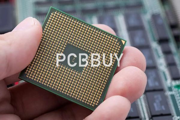
Precision laser drilling creates microvias with diameters as small as 75μm, perfectly suited for fine-pitch BGA and CSP packages.
4. Copper Filling and Electroplating
Copper is electrochemically deposited into vias, filling the internal volume and coating the surface with uniform copper for optimal conductivity.
5. Outer Layer Imaging and Etching
Outer circuit layers are imaged and etched to form the final wiring pattern, with critical attention to impedance and signal integrity.
6. Surface Finishing and Testing
Final finishes (ENIG, OSP, Immersion Silver, etc.) are applied before 100% E-testing and AOI inspection.
Quality Assurance: How PCBBUY Maintains Excellence
Our factory adheres to IPC Class 2/3 standards and operates under ISO 9001, UL, RoHS certifications. We deploy:
-
AOI for each layer
-
In-process and final electrical testing
-
X-ray analysis for via integrity
-
Impedance and thermal shock testing
These systems ensure every HDI PCB meets tight mechanical, electrical, and reliability requirements.
Why Choose PCBBUY as Your HDI PCB Factory Partner?
-
10+ Years of HDI Experience
-
Rapid prototyping and scalable mass production
-
Engineering support with free DFM and stack-up guidance
-
Competitive pricing and global delivery
-
Strong emphasis on quality and communication

Frequently Asked Questions (FAQ)
Q1: What is the difference between HDI and standard PCBs?
HDI PCBs feature finer lines/spaces, smaller vias, and higher connection pad density compared to standard PCBs, enabling compact, high-speed designs.
Q2: Can PCBBUY support via-in-pad and stacked vias?
Yes. Our laser drilling and copper-filling processes allow for via-in-pad, stacked, and staggered via designs.
Q3: What’s the typical lead time for HDI PCB production?
Depending on complexity, prototypes can be delivered in 5–7 working days. Mass production takes 10–15 days.
Q4: What materials are available for HDI builds?
We offer FR-4, high-Tg, halogen-free, and CTI-compliant substrates based on customer specs.
Q5: How does PCBBUY ensure via reliability?
We use automated electroplating with strict process controls, X-ray via inspection, and thermal cycling tests.
Industry Category


