Mastering the HDI PCB Manufacturing Process
By:PCBBUY 06/26/2025 17:10
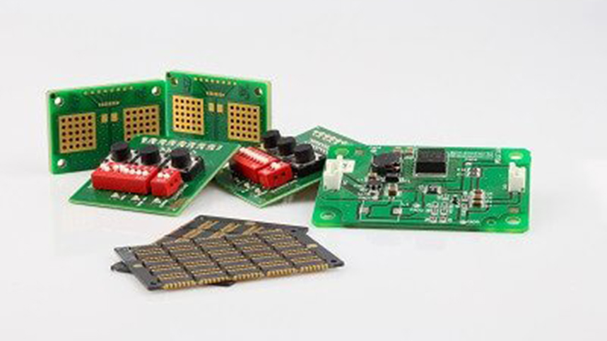
Why Understanding the HDI PCB Manufacturing Process Matters?
As electronics become increasingly compact and powerful, High-Density Interconnect (HDI) PCBs have emerged as the backbone of advanced technology. Whether you are building next-gen smartphones, IoT devices, or aerospace applications, understanding the HDI PCB manufacturing process is critical to achieving both performance and reliability.
PCBBUY, a leading global PCB manufacturer, is proud to offer cutting-edge HDI PCB solutions tailored to meet the most demanding requirements. In this guide, we outline the full spectrum of PCBBUY's HDI capabilities, step-by-step processes, and the engineering standards we maintain to ensure superior quality.
1. HDI PCB Material Selection
|
Item |
Standard |
Remarks |
|
Material |
FR-4 |
TG135–TG170, halogen-free and CTI materials available upon request |
At PCBBUY, we use industry-proven materials like FR-4 for standard HDI builds, while also offering high-Tg, halogen-free options for high-performance applications. Customized dielectric materials are also available based on impedance or CTI needs.
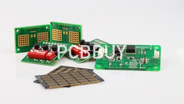
2. HDI Layer Count and Stack-Up Options
|
Item |
Standard |
Remarks |
|
Number of Layers |
1st Order: 4-10 layers2nd Stage: 6-10 layers |
Custom stack-ups available |
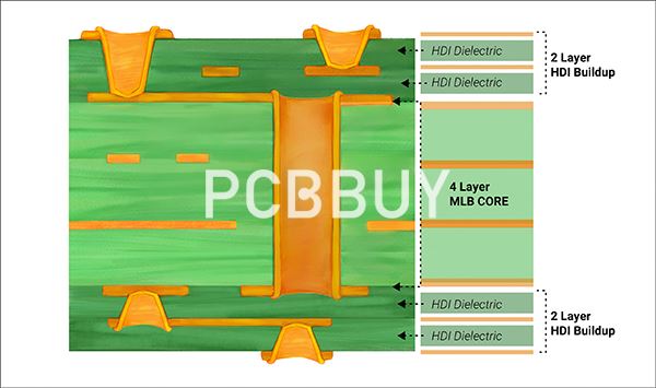
From basic 1+N+1 to more advanced 2+N+2 constructions, PCBBUY supports multi-layer HDI PCB builds. Our engineers help you optimize layer configurations for signal integrity, cost, and thermal reliability.

3. Advanced Construction Types
|
Item |
Standard |
Remarks |
|
Construction Type |
1st order: 1+N+1, 1+1+N+1 +12nd order: 2+N+2, 1+2+N+2+1 |
Electroplated via filling available |
Our HDI stack-ups are engineered for high-density interconnects using buried and blind vias. For finer vias (≤0.3mm), we use electroplating filling processes to ensure signal continuity and mechanical reliability.
4. Trace Width Capabilities
|
Item |
Standard |
Remarks |
|
Trace Width |
2/2mil (min) |
Ideal for HDI/BGA and fine-pitch ICs |
PCBBUY leverages advanced imaging and etching technology to achieve minimum 2mil line/space designs. This enables complex routing for high-speed and RF circuits in HDI designs.
5. Blind Via Technology
|
Item |
Standard |
Remarks |
|
Blind Via |
Mechanical ≥0.15mmLaser ≥0.075mm |
Specification review required |
Our blind via drilling capabilities include high-precision laser and mechanical processes. All via geometries are reviewed and validated before fabrication to ensure manufacturability and reliability.
6. Hole Size and Registration
|
Item |
Standard |
Remarks |
|
Hole Size |
Min unilateral ≥3mil |
Custom drills possible on request |
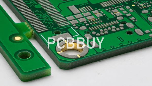
With advanced CNC and laser drills, PCBBUY achieves micro-drilling tolerances ideal for stacked via and via-in-pad structures.
7. Hole Copper Thickness
|
Item |
Standard |
Remarks |
|
Hole Copper |
>18μm (mechanical)>13μm (laser) |
Review required |
Ensuring sufficient copper thickness in vias is crucial for conductivity and reliability. PCBBUY uses tightly controlled plating parameters to ensure IPC standards are met.
8. Via Electroplating Process
|
Item |
Standard |
Remarks |
|
Via Electroplating |
Depth: 0.05mm~0.1mmTolerance: ±15% |
Full via copper fill ensures metallization |
Using advanced electroplating systems, we fill microvias with copper to guarantee structural strength and thermal reliability. This is especially important for stacked or staggered vias in multi-order HDI designs.
Why Choose PCBBUY for HDI PCB Manufacturing?
-
Customized HDI Stack-Ups: We support all mainstream and specialized configurations.
-
Precision Laser Drilling: For clean microvias down to 0.075mm.
-
LDI & Fine-Line Imaging: Accurate 2/2mil trace widths.
-
Advanced Plating Lines: Ensure copper fill, reliability, and consistent via quality.
-
Global Delivery & Support: From prototyping to mass production.

Conclusion
Understanding the HDI PCB manufacturing process allows engineers and product managers to make smarter design and sourcing decisions. With PCBBUY's proven manufacturing expertise and a commitment to advanced technology, we’re here to bring your HDI designs to life with speed, precision, and reliability.
Industry Category


