PCB Component Spacing Guide for Reliable and Manufacturable Designs
By:PCBBUY 11/27/2025 16:59

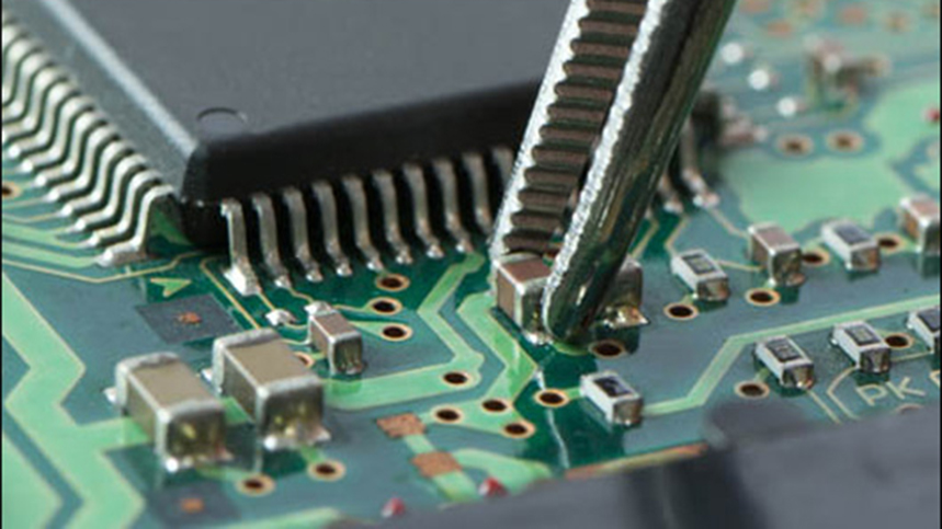
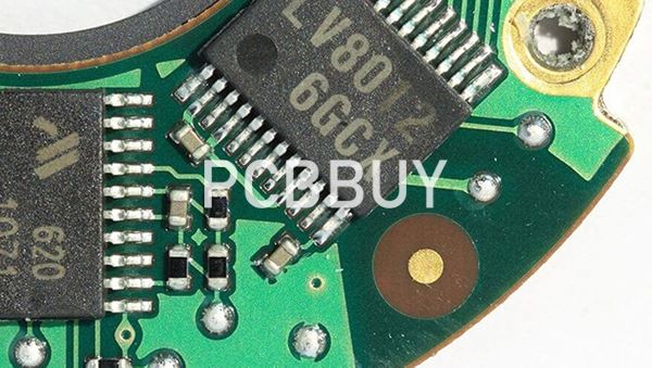
PCB component spacing is a critical factor in determining manufacturability, electrical integrity, thermal behavior, and overall system reliability. As PCB designs transition toward higher component density—driven by HDI structures, fine-pitch packages, and miniaturized passive components—spacing requirements must be evaluated from both an electrical and process-capability standpoint.
At PCBBUY, we work with thousands of global customers every year, and improper component spacing is one of the most common issues we help correct during DFM reviews. In this article, we break down why PCB component spacing matters, the key guidelines you should follow, and how PCBBUY’s manufacturing capabilities support high-density layouts.
Why PCB Component Spacing Matters
1. Manufacturability and SMT Yield
When components are placed too close, several problems may occur:
-
Solder paste bridging during reflow
-
AOI inspection difficulty
-
Rework and repair challenges
-
Insufficient room for pick-and-place nozzles
PCBBUY’s high-precision SMT lines can handle fine-pitch packages, but proper spacing always makes production smoother, faster, and more reliable.

2. Electrical Performance
PCB component spacing affects:
-
Crosstalk between high-speed signals
-
EMI/EMC compliance
-
Impedance stability
-
Noise coupling in analog circuits
Well-planned spacing reduces interference and ensures cleaner, more predictable performance.
3. Thermal Behavior & Reliability
High-power components require enough spacing for:
-
Heat dissipation
-
Airflow
-
Stress reduction during thermal cycling
Too tight spacing often leads to premature component failure.

Standard PCB Component Spacing Guidelines
While exact values depend on board type and component size, the following general rules apply:
Passive Components
|
Component Size |
Minimum Spacing |
|
0201 |
≥ 0.10–0.15 mm |
|
0402 |
≥ 0.15–0.20 mm |
|
0603 |
≥ 0.20–0.25 mm |
|
0805+ |
≥ 0.25–0.50 mm |
IC Packages
-
QFN/QFP: Maintain at least 0.5–1.0 mm courtyard spacing
-
BGA: Depends on pitch, but typically 0.2–0.4 mm between adjacent BGAs
-
Fine-pitch BGA (0.3–0.4 mm pitch): Requires controlled spacing + X-ray inspection
High-Voltage Isolation
Follow creepage/clearance rules:
-
Up to 30V: 0.1–0.2 mm
-
30–250V: 0.5–2.0 mm
-
250V+: 3–8 mm depending on the standard

How Manufacturing Capabilities Affect Component Spacing?
At PCBBUY, spacing recommendations come not just from design theory but from real production experience. Our SMT and PCB fabrication technologies determine the safe spacing we can support:
High-Precision Pick-and-Place Machines
Supports 0402 / 0201 components with consistent accuracy.
Laser-Cut Stencils with Nano-Coating
Better paste release improves spacing capability for fine-pitch pads.
Reflow Thermal Profiling
Ensures solder paste stabilization even for tightly packed components.
AOI + X-ray Inspection
Critical for:
-
Dense QFN
-
Fine-pitch BGA
-
Stacked components
HDI PCB Fabrication
Microvias, resin-filled vias, and fine trace/space allow optimal routing between tight components.
Best Practices for PCB Component Spacing
-
Keep enough courtyard clearance for inspection and rework.
-
Avoid placing tall components next to very small ones.
-
Keep high-speed or high-voltage areas isolated.
-
Do not block airflow around power devices.
-
Provide enough space for test points and probes.
-
Always run a DFM check before manufacturing.
PCBBUY offers free DFM support to help designers catch spacing issues early, ensuring fast, trouble-free production.

Why Choose PCBBUY for High-Density PCB Assembly?
-
Advanced SMT lines supporting fine-pitch ICs and 0201 components
-
HDI PCB capabilities with laser drilling and tight tolerance control
-
IPC-certified engineers reviewing all spacing & layout concerns
-
AOI + X-ray for 100% quality assurance
-
One-stop PCB + PCBA manufacturing
-
Free DFM before production
If your project involves high-density layout requirements, PCBBUY can help you optimize spacing for both manufacturability and performance.
Conclusion
PCB component spacing plays a much bigger role than most designers expect. Whether you’re working with high-speed signals, tight HDI layouts, or high-power circuits, following proper spacing rules helps your board perform reliably and ensures smooth assembly.
PCBBUY’s engineering team is ready to assist with spacing guideline checks, manufacturability review, and high-density PCB production—simply send us your Gerber and BOM to get started.
FAQ
1. What is PCB component spacing?
PCB component spacing refers to the minimum distance between components to ensure reliable manufacturing, operation, and repair.
2. Why is component spacing important in SMT assembly?
Proper spacing prevents solder bridging, improves AOI inspection, and increases production yield.
3. How much spacing do 0402 and 0603 components need?
Typically:
-
0402: 0.15–0.20 mm
-
0603: 0.20–0.25 mm
4. What spacing is required for BGA packages?
Spacing depends on the BGA pitch but commonly ranges from 0.2–0.4 mm.
5. Can PCBBUY support high-density layouts?
Yes. PCBBUY supports HDI, fine-pitch BGA, 0201 components, microvias, and controlled impedance with full AOI + X-ray inspection.
Industry Category


