PCB manufacturing process
By:PCBBUY 04/28/2021 17:54

PCB is one of the important components in the electronic industry. Recent years, various CAD printed circuit board application software has been popularized and promoted in the industry, in the specialized PCB manufacturers, mechanization, automation production has completely replaced the manual operation.
Printed circuit board has good product consistency, it can adopt standardized design, is conducive to the mechanization and automation in the production process. At the same time, the whole printed circuit board after assembly and debugging can be used as an independent spare part to facilitate the exchange and maintenance of the whole machine products. At present, printed circuit board has been extremely widely used in the production of electronic products.
The manufacturing process of a PCB is pretty extensive. Whether you a PCB manufacturer or others, steps are crucial to the development of the board. Because each step is so critical to the process, let’s take a close look at the manufacturing process of a PCB. And we are talking about the manufacturing process in the content below.
PCB manufacturing process steps
Design and Output
Before you begin manufacturing the PCB, you need to have a design of the board. These blueprints will be what you base the process off of. The design process is generally completed through computer software. Using a trace width calculator will help with a majority of the details needed for inner and external PCB layers.
Printing the Inner Layers
The design is printed to a laminate, the body of the structure. A photo-sensitive film made from photo-reactive chemicals that will harden when exposed to ultraviolet light overs the structure.. This will help align the blueprints and the actual print of the board. Holes are drilled into the PCB to help with the alignment process.
Removing Unwanted Copper
Now, it is time to remove any unwanted copper that remained on the board. A chemical solution, similar to the alkaline solution, eats away at the unwanted copper. The hardened photoresist remains intact.
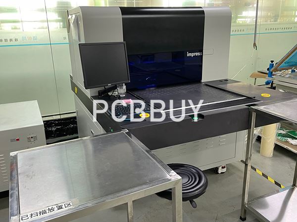
Inspection
The newly-cleaned layers will need to be inspected for alignment. The holes drilled earlier help align the inner and outer layers. An optical punch machine drills a pin through the holes to keep the layers lined up. After the optical punch, another machine will inspect the board to ensure there are no defects. From here on out, you will not be able to correct any missed errors.
Laminating the Layers
Now, you will see the board take shape as the layers are fused together. Metal clamps hold the layers together as the laminating process begins. A prepreg layer goes on the alignment basin. Then, a layer of substrate goes over the prepreg followed by a copper foil layer and more prepreg resin. Lastly, there is on more copper layer applied, which is the press plate.
Pressing the Layers
A mechanical press is then used to press the layers together. Pins are punch through the layers to keep them properly aligned and secured, these pins can be removed depending on the technology. If correct, the PCB will go to the laminating press, which applies heat and pressure to the layers. The epoxy melts inside of the prepreg that, along with the pressure, fuses the layers together.
Drilling
Holes are drilled into the layers by a computer-guided drill to expose the substrate and inner panels. Any remaining copper after this step is removed.
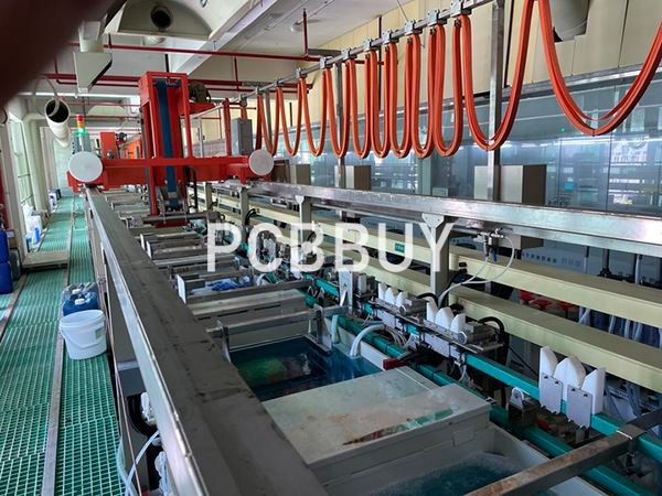
Plating
The board is now ready to be plated. A chemical solution fuses all of the layers together. The board is then thoroughly cleaned by another series of chemicals. These chemicals also coat the panel with a thin copper layer, which will seep into the drilled holes.
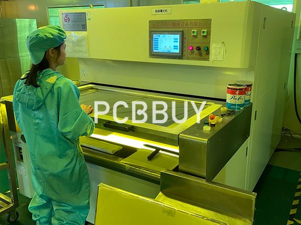
Outer Layer Imaging
Next, a layer of photoresist, similar to Step 3, is applied to the outside layer before being sent for imaging. Ultraviolet light hardens the photoresist. Any undesired photoresist is removed.
Etching
The same chemical solution from before removes any unwanted copper under the resist layer. The tin guard layer protects the needed copper. This step established the PCB’s connections.
Solder Mask Application
All of the panels should be cleaned before the solder mask is applied. An epoxy is applied with the solder mask film. The solder mask applies the green color you typically see on a PCB. Any unwanted solder mask is removed with ultraviolet light, while the wanted solder mask is baked on to the board.
Silk screening
Silk screening is a vital step since this process is what prints critical information onto the board. Once applied, the PCB passes through one last coating and curing process.
Surface Finish
The PCB is plated with either a solderable finish, depending on the requirements, which will increase the quality/bond of the solder.
Testing
Before the PCB is considered complete, a technician will perform an electrical test on the board. This will confirm the PCB functions and follows the original blueprint designs.
Assembly
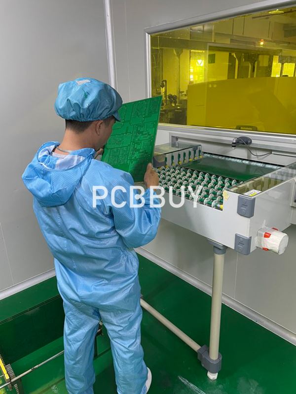
In assembly the bare board is populated with electronic components to form a functional printed circuit assembly (PCA), sometimes called a PCBA. In through-hole technology, the component leads are inserted in holes surrounded by conductive pads; the holes keep the components in place. In both through hole and surface mount, the components are then soldered; once cooled and solidified, the solder holds the components in place permanently and electrically connects them to the board.
Protection and packaging
PCBs intended for extreme environments often have a conformal coating, which is applied by dipping or spraying after the components have been soldered. The coat prevents corrosion and leakage currents or shorting due to condensation. The earliest conformal coats were wax; modern conformal coats are usually dips of dilute solutions of silicone rubber, polyurethane, acrylic, or epoxy. Another technique for applying a conformal coating is for plastic to be sputtered onto the PCB in a vacuum chamber. The chief disadvantage of conformal coatings is that servicing of the board is rendered extremely difficult
Industry Category


