PCB layers
By:PCBBUY 04/26/2021 18:12

Before we are talking about PCB layers, it is necessary to have a clear perception of layers. All the layers are responsible for assembly or building a PCB, and they are the basic of PCB.
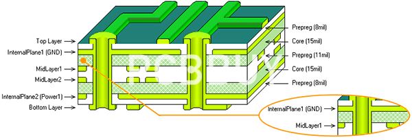
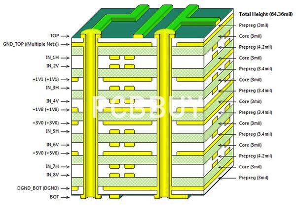
A layer is the signal conducting levels that are vertical to the PCB plane. And you’ll find a 2-layer PCB having a top and bottom layer. For a 4-layer PCB, for instance, you’ll find a top, inner 1, inner 2, and bottom layer. And the same thing applies for other PCB layers.
Generally, regular PCBs consist of solder masks on the outer copper layer. And you can find the solder masks on both the top and bottom copper layers. Besides, the solder masks get applied either as liquid or as a sheet on the PCB layers. Plus, they have printed openings with a subtractive photographic procedure.
Overall, PCB layers are the foundation blocks of a PCB. So, they include the copper, the dielectric material, and one more thing. And it’s the trace dimensions aligned with the dimension or mechanical layer.
If you want to order PCB product, please check and custom your order online.
PCB layers tutorials
There are 3 kinds of tutorials that make the PCB layers complete:
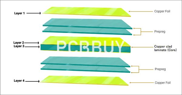
Dielectric materials
The dielectric materials offer two critical functions for PCBs. And all that happens as the PCBs run rapid signals. The dielectric materials help to isolate signals on adjacent PCB layers. The stability of a PCB highly depends on the steady impedance of dielectric materials.
Copper
The various weight and thickness of copper in a PCB impacts too. Of course, it influences the capacity of the PCB to attain the right amount of current flow. Also, it helps to describe the amount of current loss. The quality of copper in a PCB impacts the impedance of a ground plane. Besides, it affects the power plane’s thermal conductivity.
Trace Dimensions
They help to provide PCB foundational measurements. Besides, the assembly information helps to regulate the location and mounting of electronic devices.
What are the types of PCB layers?
By numbers
Usually, the layers in the PCB are so tightly integrated, so it's not always easy to see the actual number, but if you look closely at the motherboard, you can see it.
PCB board has the following three main types of division:
Single-layered boards
On the most basic PCB, the parts are concentrated on one side and the wires on the other. This type of PCB is called a single panel because the wire appears on only one side.
Double-layered boards
This board has wiring on both sides, but to use the wiring on both sides, there must be a proper electrical connection between the two sides. This "bridge" between circuits is called a guide hole. A guide hole is a small hole in a PCB filled or coated with metal that can be connected to wires on both sides.
In order to increase the area that can be wired, multi-layered board uses more single or double-sided wiring boards. With a double lining, two one-way for outer layer or two double lining, two blocks of single outer layer of the printed circuit board, through the positioning system and alternate insulation adhesive materials and conductive graphics interconnection according to design requirement of printed circuit board becomes four, six layer printed circuit board, also known as multilayer printed circuit board.
By function
Mechanical Layer
The function of a mechanical layer is to reveal information about the PCB assembly methods and printing. So, you can choose to have more than one mechanical layer. It can be a complicated shape or a simple rectangle.
Overlay / Silkscreen Layers
The Silkscreen layer consists of the Bottom and Top overlay. And it’s useful for putting text information. Besides, it’s crucial to get separate files, for the fabricator, to the bottom and top overlays.
Routing Layers
Routing layers are in the internal and external parts of a PCB. Also, it’s a layer that designers took time to perfect. Plus, it’s useful for component interconnection. Before you create your board, it’s necessary to provide the routing layers to your fabricator.
Solder Mask Layers
A solder mask layer is what you see when you hold a PCB. That is, it’s a thin green protective covering. And it usually helps to cover the board’s top and bottom. If there’s debris on your board, this board will help you protect traces from shorting.
Solder Paste Layers
A solder paste comes in handy when you have surface mounts components. So, this layer helps to bond the component pin to the surface (copper) of your board. Also, it improves the flow of the solder.
Keep Out Layer
This layer shows the limit of the working area of your board design. It will show if there’s any violation of the pre-set boundaries.
Wanna know PCB knowledge? Check and read for more.
Industry Category


