Precision Manufacturing of Epoxy Filled Vias in PCB
By:PCBBUY 07/21/2025 15:57
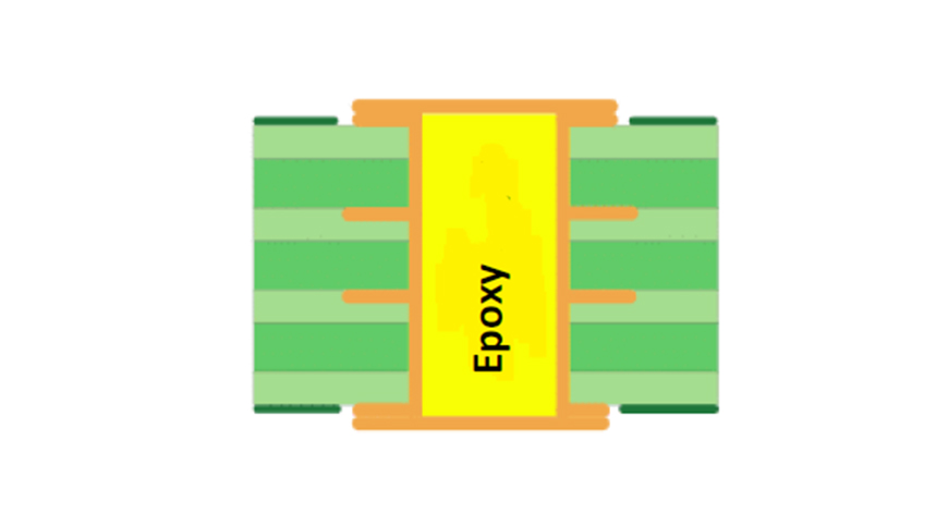
Introduction to Epoxy Filled Vias in PCB Manufacturing
In high-density interconnect (HDI) PCB design, epoxy filled vias play a vital role in enhancing performance, mechanical strength, and design flexibility. As a leading epoxy filled vias PCB manufacturer, PCBBUY specializes in delivering high-reliability HDI solutions that meet rigorous electronic packaging requirements. This article explores the critical process parameters, equipment capabilities, and engineering standards that define our epoxy via filling process.
Why Choose Epoxy Filled Vias?
1. Structural Integrity and Planarity
Epoxy filling reinforces the via structure and creates a flat surface for component mounting—essential in BGA, QFN, and CSP applications. At PCBBUY, we utilize Zhuyou epoxy ink, a trusted industry-grade material known for its thermal resistance and mechanical durability.
2. Isolation and Conductivity Control
Epoxy filled vias ensure no solder migration during assembly and prevent contamination from plating solutions. They also maintain uniform impedance and excellent dielectric strength—key advantages for signal integrity in HDI PCBs.
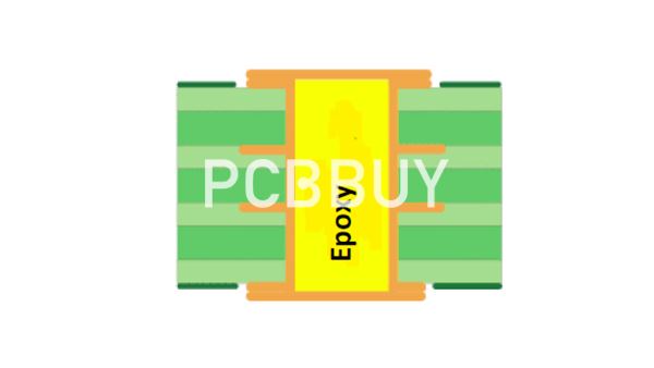
PCBBUY’s Epoxy Filled Vias Process Standards
PCBBUY follows strict internal quality standards to ensure every epoxy filled via performs reliably in complex multilayer boards. Below are our key technical parameters:
|
Item |
Standard |
Remarks |
|
Ink |
Zhuyou epoxy ink |
Consistent quality for high-density builds |
|
Board Size |
≤650 mm length |
Oversized panels require custom evaluation |
|
Board Thickness |
0.2 mm – 8.0 mm |
Flexible support for various applications |
|
Plugged Via Hole Size |
0.2 mm – 1.0 mm |
Oversize requires additional assessment |
|
Hole Range Tolerance |
≤0.2 mm difference between adjacent vias |
Ensures consistent resin flow and pressure stability |
|
Hole Sunken Parameters |
≤0.4 mm vias: ≤5 μm / ≤15 μm; >0.4 mm: ≤50 μm |
Tighter controls available on request; zero sag requires requalification |
Step-by-Step Epoxy Via Filling Process at PCBBUY
Step 1: Via Drilling and Desmearing
Precision mechanical or laser drilling defines microvia geometry. A desmear process follows to ensure proper epoxy adhesion.
Step 2: Epoxy Injection and Vacuum Filling
We inject Zhuyou epoxy under controlled pressure and vacuum conditions to eliminate air bubbles and voids.
Step 3: Curing and Hardening
Filled vias are oven-cured at controlled temperature ramps to ensure complete polymerization and dimensional stability.
Step 4: Surface Grinding and Planarization
We perform controlled surface grinding (sanding or planarization) to create a perfectly flat, solderable surface—especially critical under SMT pads or BGA footprints.
Step 5: Quality Control and Cross-section Analysis
Using AOI, X-ray, and microsection techniques, we verify filling quality, no voids, and depth consistency across multiple via sizes.

Advantages of PCBBUY’s Epoxy Filled Via Capabilities
-
✅ Customizable specs for hole size, ink, sunken depth
-
✅ Full technical review for out-of-range designs
-
✅ Compatibility with HDI stack-ups, buried vias, and via-in-pad
-
✅ On-time delivery with full in-process QA/QC
Whether you're designing ultra-compact consumer devices or aerospace-grade circuit boards, PCBBUY’s epoxy filled via process ensures long-term reliability and electrical performance.
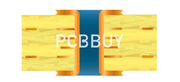
Frequently Asked Questions (FAQ) about Epoxy Filled Vias
Q1: What is the main difference between epoxy filled vias and via tenting?
A1: Epoxy filled vias are completely sealed with resin and cured for strength, while tented vias are only covered with solder mask—less reliable for high-density boards.
Q2: What applications typically require epoxy filled vias?
A2: Epoxy filled vias are used in BGA pad designs, via-in-pad structures, HDI PCBs, and boards requiring high mechanical strength or reflow resistance.
Q3: Can PCBBUY customize epoxy filling tolerances or materials?
A3: Yes. Our engineering team can review and support customization requests beyond standard hole sizes, tolerances, or ink brands, especially for IPC Class 3 projects.
Q4: What inspection methods are used for epoxy via quality?
A4: We use automated optical inspection (AOI), X-ray imaging, and cross-sectional analysis to validate epoxy distribution and via coverage.
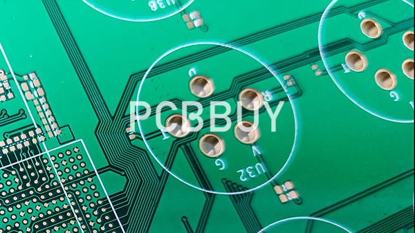
Conclusion
PCBBUY stands out as a top-tier epoxy filled vias PCB factory, offering precise control over critical dimensions, filling depth, and resin quality. Our flexible manufacturing approach and adherence to industry-leading standards allow customers to push design boundaries without compromising performance.
If you're looking for a reliable partner with scalable HDI production capabilities, contact PCBBUY today to get a quote or discuss your next high-density project.
Industry Category


