Understanding HDI PCB Cost in Cost-Effective HDI Manufacturing
By:PCBBUY 06/24/2025 16:43
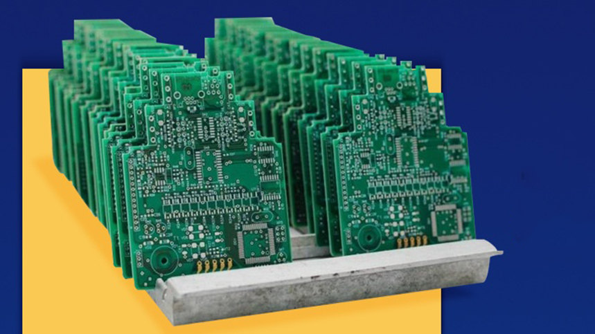
As the demand for miniaturized and high-performance electronics increases, HDI (High-Density Interconnect) PCBs have become essential across industries like mobile devices, automotive, medical, and aerospace. However, one of the most common questions engineers and procurement teams face is:
What exactly drives HDI PCB cost?
In this article, PCBBUY explores the critical cost factors behind HDI PCB fabrication, including layer structure, materials, microvia processing, and copper plating—offering insights into how our advanced production capabilities help customers achieve high reliability at competitive prices.
What Determines the Cost of an HDI PCB?
1. Layer Count & Stack-Up Strategy
At PCBBUY, our HDI stack-up solutions range from:
-
1st Order HDI: 4–10 layers (1+N+1, 1+1+N+1+1)
-
2nd Order HDI: 6–10+ layers (2+N+2, 1+2+N+2+1)
Higher layer counts and staggered or stacked via designs significantly increase lamination cycles, alignment complexity, and inspection requirements—directly affecting the cost.
Pro Tip: Keeping to a 1st-order HDI layout can reduce up to 25% in production cost for mobile and wearable devices.
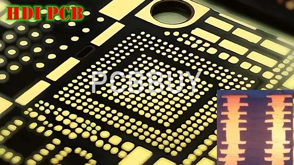
2. Construction Type: Via Structure Design
PCBBUY supports both mechanical and laser via configurations:
|
Construction Type |
Example Layout |
Via Size Support |
|
1st Order HDI |
1+N+1, 1+1+N+1+1 |
Buried vias ≤ 0.3mm |
|
2nd Order HDI |
2+N+2, 1+2+N+2+1 |
Stacked microvias ≤ 0.3mm |
Our engineers help customers choose between mechanical blind via and laser-drilled blind via based on electrical performance, density, and budget.

3. Minimum Trace & Spacing
With a minimum line/space capability of 2/2mil, PCBBUY ensures compact designs without sacrificing signal integrity. However, the finer the lines, the more advanced the etching and imaging equipment required, increasing cost.
Cost-saving tip: Slightly widening trace/space to 3/3mil can reduce HDI PCB cost by 10–15%.
4. Via & Hole Processing
Blind Via Capabilities:
|
Type |
Min Size |
|
Mechanical Blind Via |
≥ 0.15mm |
|
Laser Blind Via |
≥ 0.075mm |
Via Filling & Electroplating:
-
Laser via plating depth: 0.05mm–0.1mm
-
Tolerance: ±15%
-
Copper-filling: Ensures via pad flatness for via-in-pad designs
Advanced electroplating adds complexity but is essential for reliability and conductivity in HDI boards.
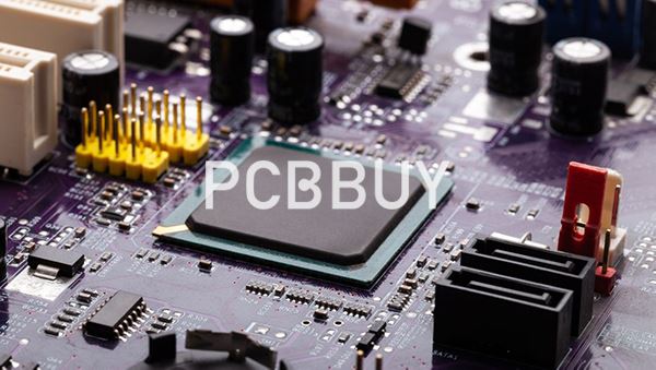
5. Material and Copper Specification
Material Options:
-
Base: FR-4
-
Optional: TG135–TG170, halogen-free, CTI-rated materials
Hole Copper Thickness:
-
No laser blind: >18μm
-
Laser blind: >13μm
Using high-Tg, low-loss materials and ensuring proper copper distribution affects signal quality and thermal performance—but also impacts material costs.
6. Summary Table: PCBBUY HDI PCB Core Capabilities
|
Feature |
Capability |
|
Layer Count |
4–10 layers (expandable) |
|
Trace Width |
2mil minimum |
|
Blind Via |
Mech ≥ 0.15mm / Laser ≥ 0.075mm |
|
Hole Size |
Unilateral ≥ 3mil |
|
Hole Copper |
Mech >18μm / Laser >13μm |
|
Via Plating Depth |
0.05–0.1mm (±15%) |
How PCBBUY Helps You Optimize HDI PCB Cost?
-
Early Design Reviews: We offer free DFM analysis to help reduce excessive stack-ups or avoid overuse of via-in-pad
-
Transparent Pricing: Online quoting system provides instant visibility into price drivers
-
In-House Laser & LDI Facilities: Shortens lead time and reduces outsourcing markup
-
Flexible MOQ: We support small batches for prototypes without high NRE charges
Typical HDI PCB Cost Range at PCBBUY
|
Type |
Avg. Cost (USD/m²) |
Notes |
|
1st Order HDI |
$80–$130/m² |
Smartphones, wearable devices |
|
2nd Order HDI |
$150–$230/m² |
IoT, automotive, industrial |
|
Advanced Stack HDI |
$250+/m² |
Military, radar, base stations |
Note: Pricing varies based on material, via structure, and surface finish.
Frequently Asked Questions (FAQ)
|
❓ Question |
✅ Answer |
|
Why is HDI PCB more expensive than standard PCB? |
Due to advanced via processing (laser drill, plating), tighter tolerances, and multi-lamination. |
|
Can I reduce HDI cost by modifying layout? |
Yes. We recommend simplifying the via structure and optimizing line/space. |
|
Does copper filling for laser vias affect price? |
Yes, via-in-pad with filling and capping adds 10–15% to the total cost. |
|
Does PCBBUY offer HDI prototyping services? |
Absolutely! We support HDI prototype and small-batch production with low MOQ. |
Contact PCBBUY for Custom HDI PCB Cost Solutions
Whether you're a startup prototyping wearables or an OEM sourcing complex HDI boards, PCBBUY is ready to support your HDI journey. With cutting-edge manufacturing lines and expert engineering support, we help you balance performance and cost effectively.
Industry Category


