What Causes High-Layer PCB Lamination Defects: Stackup Design or Process Control?
By:PCBBUY 11/12/2026 14:41
Lamination is one of the most critical stages in high-layer-count PCB manufacturing. Once multiple cores, prepregs, and copper foils are bonded into a single multilayer structure, internal defects become difficult or impossible to repair economically. Layer shifting can compromise interlayer registration, delamination can weaken the bond between dielectric and copper interfaces, and resin voids can create localized structural weaknesses inside the board.
For automotive electronics, industrial control systems, power supplies, energy storage equipment, and embodied robotics, these defects are more than manufacturing imperfections. They can become starting points for electrical opens, insulation failures, CAF-related reliability problems, and fatigue under repeated thermal cycling.
This leads to a common engineering question: Are PCB lamination defects primarily caused by stackup design or by process control?
The answer is rarely one or the other. Stackup design determines how challenging a board is to laminate, while process control determines whether the manufacturer can consistently produce that structure within an acceptable process window. Layer shifting, delamination, and resin voids are different failure modes, but they share several underlying variables: resin flow behavior during heating, the removal of trapped air and volatiles, and the dimensional response of materials under heat and pressure.
Understanding how these factors interact is essential for identifying root causes and preventing recurring defects in high-layer-count PCBs.
1. PCB Layer Shifting: How Stackup Design Increases Registration Risk
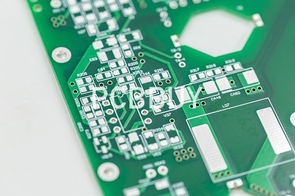
Layer shifting, also called layer misregistration or interlayer registration error, occurs when individual layers move relative to one another during lamination. It may be identified through X-ray inspection of registration targets or through measurements of layer alignment after drilling. In severe cases, the displacement can reduce annular ring margins or cause drilled holes to miss their intended inner-layer pads.
The problem is not simply that the layers were incorrectly aligned before pressing. The more important question is whether the stackup and lamination process can maintain that alignment under heat and pressure.
How lamination conditions contribute to layer shifting?
Traditional pin-based or rivet-based registration systems have mechanical clearances. When the stack is heated and pressurized, these clearances can allow small relative movements between individual cores and prepregs. If the temperature rises too quickly, the resin may enter a low-viscosity state before the stack has sufficient mechanical stability. This can reduce resistance to movement and increase the risk of layer displacement.
Pressure timing also matters. Applying pressure before the stack reaches the intended resin-flow stage can create uneven movement across the panel. Excessive or poorly timed resin flow may further affect the stability of the layer structure.
How stackup design increases the risk?
Thick-copper designs are particularly challenging because they require sufficient resin volume to fill the gaps around copper features. Depending on copper thickness, pattern density, and dielectric requirements, additional prepreg layers or a different prepreg construction may be necessary. More prepreg interfaces and a more complex material stack can make registration control more demanding.
Copper distribution is another important factor. Consider a multilayer stackup in which a high-copper-coverage plane is adjacent to a signal layer with relatively sparse copper. The difference in surface topography and local resin demand can create nonuniform flow conditions during pressing. These variations may contribute to localized shear forces and make layer alignment more sensitive to changes in the lamination cycle.
This is why registration risk should be evaluated during stackup design rather than treated only as a press-machine issue. A balanced copper distribution and a suitable prepreg selection generally provide a more manageable lamination window. A stackup with concentrated thick copper, significant copper-density differences, or a large number of prepreg sheets may require tighter control of temperature ramping, pressure timing, and material positioning.
How PCBBUY manages layer registration?
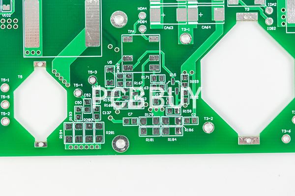
PCBBUY approaches high-layer-count PCB registration as a combined engineering and manufacturing control issue. Its stated multilayer PCB manufacturing capability covers 4–26 layers, with reported layer alignment accuracy of ±12 μm and registration accuracy of 25 μm.
LDI exposure equipment is used to control inner-layer image positioning, with a stated alignment accuracy of approximately ±10 μm. This helps reduce initial pattern-transfer errors before lamination. After pressing, X-ray inspection can be used to evaluate internal registration targets and identify layer displacement that may not be visible from the board surface.
For thick-copper designs or stackups with significant local copper-density differences, the engineering review should also examine whether the selected prepreg construction provides enough resin to accommodate the copper topography. If the structure is especially challenging, adjustments to the stackup or a sequential lamination approach may be considered where the design and manufacturing route permit.
The objective is not simply to tighten press parameters. It is to make sure the stackup is compatible with the available lamination process window.
2. PCB Delamination: Stackup Determines Bonding Potential, Process Control Determines Bond Quality
PCB delamination refers to the separation of bonded layers or interfaces within the laminate structure. It can occur at the copper-to-resin interface, between prepreg layers, or around interfaces affected by inadequate surface preparation.
The immediate problem is insufficient interfacial bonding strength. However, the underlying cause may originate in material selection, stackup design, surface preparation, moisture control, or the lamination cycle.
How stackup design affects interlayer bonding?
The stackup establishes the material conditions required to form a reliable bond. Prepreg resin content must be sufficient to wet the copper surface and fill the spaces around circuit features. Prepreg flow characteristics must also be compatible with the copper thickness and pattern density of adjacent layers.
If resin content is too low for the required fill volume, or if the glass-to-resin ratio is unsuitable for the local copper topography, certain areas may experience resin starvation. This is particularly important around thick-copper features and areas with substantial differences in copper coverage.
Material compatibility also matters. The thermal expansion behavior of the core and prepreg system affects the stress generated during heating and cooling. A poorly matched material construction may increase stress at the bonded interfaces, particularly during subsequent soldering or thermal cycling.
How the lamination process causes delamination?
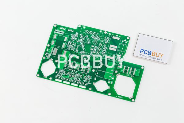
Even a well-designed stackup can delaminate if the lamination cycle is not properly controlled.
An inadequate pre-press stage may allow pressure to be applied before the resin has reached the intended flow condition. This can restrict resin movement or create uneven pressure distribution. Conversely, excessive resin flow may leave insufficient resin in critical areas after the material has moved away from the interface.
Air and volatile substances must also be removed before the resin reaches its gel stage. If the evacuation process is insufficient, trapped gas can expand during heating and create localized pressure within the stack. Moisture absorbed by cores or prepregs can produce a similar problem because water vapor may form during the lamination cycle.
Insufficient curing temperature or dwell time can also prevent the resin system from achieving its intended degree of cure. The resulting laminate may have inadequate bonding performance or reduced resistance to subsequent thermal stress.
Delamination is therefore rarely attributable to a single parameter. A stackup with limited resin-flow margin may still be manufacturable, but it requires a lamination cycle that is specifically matched to the material construction.
How PCBBUY evaluates delamination risk?
PCBBUY uses materials from established suppliers such as Kingboard and Shengyi. For more demanding multilayer products, prepreg selection and lamination profiles need to be matched to the actual stackup rather than relying on one general-purpose press recipe.
Inspection is equally important. Metallographic microsectioning allows engineers to examine internal interfaces and identify evidence of separation or incomplete bonding. Thermal stress testing provides additional information about whether the laminate can withstand elevated-temperature exposure without developing unacceptable structural defects.
PCBBUY has stated a thermal shock test condition of 288 ± 5°C for 10 seconds over three cycles. This should be understood as a specified test condition used for its relevant evaluation process, not as a universal requirement for every PCB or application. The applicable test method and acceptance criteria should be agreed upon for each product.
For automotive and industrial control applications, combining microsection analysis with thermal stress evaluation can provide more meaningful evidence of laminate integrity than relying on external visual inspection alone.
3. Resin Voids in PCB Lamination: Process Control Is Critical, but Stackup Sets the Process Window
Resin voids are localized gaps or unfilled regions within the laminate structure. They may occur between copper features, within resin-rich regions, or around areas where the resin has failed to fill the required space.
Compared with layer shifting and delamination, resin voids are often more directly associated with resin flow, vacuum performance, and pressure timing. However, stackup design still determines how much resin is required and how difficult it is to achieve complete filling.
Why resin voids form during lamination?
Resin viscosity changes significantly as the temperature increases. If the temperature rises too quickly, the available resin-flow period may be insufficient for the material to fill the required spaces and allow trapped air to escape.
Vacuum performance is another critical factor. Air trapped between layers or within the material structure must be removed before the resin gels. If the vacuum level, evacuation timing, or vacuum-hold period is inadequate, residual gas may remain inside the laminate.
Pressure timing must also match the resin system. Applying full pressure too early may restrict the escape of trapped air. Applying pressure after the resin has passed its effective flow stage may be too late to achieve adequate filling. Once the resin gels, its ability to redistribute and fill remaining gaps is greatly reduced.
These conditions explain why a stable lamination cycle must be developed around the specific resin system rather than selected only by board thickness or layer count.
How copper distribution affects resin filling?
Copper distribution determines the amount and location of resin needed during lamination.
A layer with broad, continuous copper coverage may have relatively limited surface topography. A signal layer with sparse traces, isolated pads, and large copper-free areas may contain deeper gaps between conductors. The resin must fill these spaces while maintaining the required dielectric thickness.
When these two types of layers are adjacent, the same prepreg construction may need to accommodate very different local resin demands across the panel. If the resin volume is insufficient for the actual copper topography, adjusting the temperature ramp alone may not solve the problem. Some areas may remain resin-starved even when other areas contain excess resin.
This is why resin-fill assessment should be part of the stackup review. Engineers need to consider copper thickness, copper coverage, trace geometry, prepreg resin content, and the required dielectric spacing together.
Vacuum lamination helps remove trapped air before resin flow and gelation. However, vacuum equipment cannot compensate for an unsuitable prepreg construction or insufficient resin volume. Both stackup design and process control must be addressed.
How PCBBUY controls resin voids?
PCBBUY's approach to resin-void control involves equipment capability, lamination-profile matching, and verification through microsection analysis.
Its high-layer-count lamination process uses vacuum hot pressing to help remove trapped air from the stack before the resin gels. For demanding structures, such as boards above 12 layers or designs with relatively thick inner-layer copper, vacuum lamination is incorporated into the manufacturing process according to the applicable product requirements.
After lamination, metallographic microsectioning provides direct evidence of the internal laminate structure. It allows engineers to examine resin filling, dielectric interfaces, and other internal features that cannot be reliably assessed through external visual inspection alone.
PCBBUY also reports a customized automatic vertical electroless copper line with a deep-hole capability of up to 13:1. This capability relates to subsequent hole metallization and should be evaluated separately from lamination quality. Consistent hole-wall copper deposition is important for overall multilayer PCB reliability, but it does not directly eliminate resin voids inside the laminate.
For high-reliability products, the inspection plan should therefore distinguish between laminate defects and plated-hole defects. Microsection analysis is particularly important because it can reveal internal conditions that electrical continuity testing may not detect.
4. Stackup Design vs. Lamination Process Control: Where Does Each Defect Originate?
Although layer shifting, delamination, and resin voids may appear together, their dominant contributing factors are not identical. The following comparison can help engineers organize the initial root-cause investigation.
| Defect | Main stackup-related factors | Main process-related factors | Recommended verification |
|---|---|---|---|
| Layer shifting | Copper imbalance, thick-copper distribution, prepreg construction, complex stackup | Registration method, temperature ramp, pressure timing, material movement | Post-lamination X-ray registration inspection and dimensional analysis |
| Delamination | Insufficient resin content, material compatibility, copper surface condition, moisture-sensitive materials | Inadequate evacuation, incorrect resin flow, insufficient curing, poor moisture control | Microsection analysis and appropriate thermal stress testing |
| Resin voids | Insufficient resin volume, uneven copper distribution, unsuitable prepreg selection | Inadequate vacuum, incorrect pressure timing, unsuitable temperature ramp, premature gelation | Microsection analysis and process-profile review |
The comparison highlights an important distinction: stackup design determines the manufacturing challenge, while process control determines how consistently that challenge can be managed. A process adjustment may reduce the occurrence of a defect, but it cannot always compensate for a fundamentally unsuitable material construction.
5. How Should Engineers Investigate PCB Lamination Defects?
When a high-layer-count PCB shows layer shifting, delamination, or resin voids, the investigation should begin with the stackup and then move into the lamination process.
The first step is to determine whether the design is manufacturable with the selected materials. Engineers should review copper distribution, finished copper thickness, prepreg resin content, dielectric thickness, and the relationship between adjacent layers. Thick-copper regions and significant copper-density differences deserve particular attention because they can increase local resin-flow demands.
The next step is to review material condition and preparation. Core and prepreg storage, handling, and moisture exposure should be checked against the material supplier's requirements. Copper surface treatment and cleanliness should also be verified because contamination or inadequate bonding treatment can weaken the interface.

The lamination records should then be reviewed. Relevant parameters include the temperature ramp, vacuum level and timing, pressure sequence, resin-flow stage, curing temperature, and dwell time. These values should be evaluated against the actual resin system and stackup rather than treated as universal settings.
Finally, inspection results should be correlated with the process records. X-ray inspection can identify registration problems, while microsection analysis can reveal internal interfaces and voids. Thermal stress testing can provide additional evidence of structural integrity under the specified test conditions.
A useful root-cause investigation does not stop when defective boards have been screened out. It should determine why the process window was insufficient for the stackup and what changes are needed to prevent recurrence.
6. How Should Buyers Evaluate a High-Layer PCB Manufacturer's Lamination Capability?
Maximum layer count alone is not a reliable measure of a manufacturer's high-layer-count PCB capability. A supplier may be able to fabricate a board with a large number of layers, but that does not automatically demonstrate consistent control of registration, resin filling, or interlayer bonding.
A more meaningful evaluation examines the engineering review and inspection evidence behind the manufacturing process.
| Evaluation area | What buyers should request | Why it matters |
|---|---|---|
| Stackup engineering | DFM review covering copper balance, resin-fill requirements, prepreg selection, and dielectric construction | Confirms that the proposed stackup is suitable for the manufacturing process |
| Layer registration | Post-lamination X-ray inspection data and registration measurements | Shows whether internal layer alignment is controlled |
| Laminate integrity | Microsection images and inspection records | Provides direct evidence of internal interfaces and resin filling |
| Thermal reliability | Thermal stress test method, conditions, and results | Helps assess structural stability under the specified thermal exposure |
| Process traceability | Relevant lamination records and corrective-action documentation | Helps identify process variation and prevent recurring defects |
PCBBUY's stated manufacturing and inspection resources include X-ray inspection, metallographic microsection equipment, four-wire low-resistance testing, and thermal stress testing. These methods address different aspects of PCB quality. X-ray inspection is used for internal registration assessment, microsectioning examines laminate and plated-hole structures, and electrical testing evaluates relevant conductive paths.
For automotive electronics, industrial control, power systems, energy storage, and embodied robotics, buyers should consider requesting first-article inspection records and agreed reliability test results before approving volume production. The exact sampling plan and acceptance criteria should be defined in the purchase specification or technical agreement.
FAQ
Should engineers investigate the stackup or the lamination process first?
Start by reviewing whether the stackup is manufacturable. Copper imbalance, insufficient resin-fill allowance, unsuitable prepreg selection, and material moisture can create structural risks before the board enters the press. If these conditions are not addressed, process optimization may only reduce the defect rate without eliminating the underlying problem.
Once the stackup has been reviewed, examine the lamination records, including the temperature ramp, vacuum sequence, pressure timing, and curing conditions. This sequence helps distinguish a design-related limitation from a process-control failure.
Can changing PCB manufacturers eliminate delamination?
Changing manufacturers does not automatically eliminate delamination. If the original failure was caused by insufficient resin volume, unsuitable material selection, or moisture absorbed by the incoming materials, the same stackup may remain vulnerable at another factory.
A qualified manufacturer should review the original stackup, inspect the material construction, and evaluate the lamination profile before starting production. First-article microsection analysis and appropriately specified thermal stress testing can help establish whether the revised process is suitable for volume manufacturing.
How are resin voids evaluated for PCB acceptance?
There is no single void-size limit that applies to every type of PCB void and every product class. Acceptance depends on the defect location, whether the void is within the laminate or a plated hole, its effect on dielectric integrity or conductor spacing, and the applicable performance specification.
IPC-6012F defines qualification and performance requirements for rigid printed boards, while IPC-A-600 provides visual interpretation of acceptable and nonconforming conditions. The applicable revisions, product class, design requirements, and any customer-specific criteria should be stated in the procurement documentation.
For this reason, buyers should avoid using a general statement such as "IPC Class 3 compliant" as a substitute for a clearly defined inspection and acceptance plan.
Can X-ray inspection detect all lamination defects?
No. X-ray inspection is useful for evaluating internal layer registration and certain structural features, but it should not be treated as a universal method for detecting delamination or resin voids.
Microsectioning is more suitable for directly examining internal laminate interfaces and localized void conditions in the sampled area. Thermal stress testing can provide additional information about structural integrity under defined test conditions. These methods complement one another rather than replace one another.
What should buyers check when qualifying a high-layer-count PCB supplier?
Buyers should look beyond the maximum layer count and ask how the manufacturer reviews stackup manufacturability, controls internal registration, verifies resin filling, and evaluates laminate integrity.
Evidence such as stackup DFM records, post-lamination X-ray measurements, microsection images, thermal stress test results, and traceable process documentation provides a more useful basis for supplier qualification than a capability statement alone.

Conclusion
The root causes of layer shifting, delamination, and resin voids in high-layer-count PCBs cannot be reduced to a choice between stackup design and lamination process control.
Stackup design determines the resin-flow demands, registration sensitivity, material compatibility, and overall difficulty of the lamination process. Process control determines whether the manufacturer can maintain the required temperature, vacuum, pressure, and curing conditions within a stable manufacturing window.
A copper-balanced stackup with an appropriate prepreg construction is easier to laminate consistently. However, even a well-designed structure can fail if the lamination cycle is poorly controlled. Likewise, a highly optimized press recipe cannot reliably compensate for insufficient resin volume or an unsuitable material combination.
For PCB engineers, the most effective prevention strategy is to include copper balance, resin-fill assessment, prepreg selection, and material compatibility in the initial DFM review. For procurement teams, supplier qualification should focus on documented stackup reviews, post-lamination registration data, microsection evidence, and application-specific reliability testing.
PCBBUY combines high-layer-count PCB manufacturing, vacuum lamination, X-ray registration inspection, microsection analysis, and thermal stress evaluation to support demanding multilayer designs. For automotive, industrial, power, energy storage, and robotics applications, the goal is not simply to manufacture more layers. It is to maintain internal alignment and laminate integrity consistently enough to support the reliability requirements of the finished product.
Industry Category