Why Is Resin Plugging Essential for Blind and Buried Vias in High-Layer-Count PCBs?
By:PCBBUY 11/20/2026 16:11
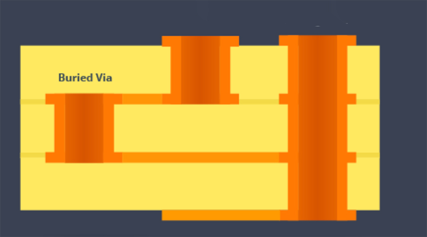
When you receive a high-layer-count PCB, you cannot see the buried vias from either the front or back of the board. They are hidden between the layers and do not participate in visual inspection. Flying probe continuity testing may not reveal their actual condition, either. Yet these invisible vias can determine whether the board maintains reliable interlayer connections after multiple lamination cycles, reflow soldering, temperature cycling, and long-term electrical operation—or develops cracks, delamination, or intermittent electrical connections at a point of stress concentration.
Whether blind and buried vias require resin plugging is not simply a process selection question that can be left open for discussion. In high-layer-count PCB structures, it is first and foremost a structural requirement. If the holes remain hollow, subsequent lamination, plating, soldering, and long-term environmental stresses can each turn those internal voids into potential failure points.
This article explains the engineering reasons behind resin plugging and the level of quality required, drawing on Lieban's manufacturing capabilities and outgoing quality standards for high-layer-count and HDI PCBs.

1. First, Understand the Different Process Constraints of Buried and Blind Vias
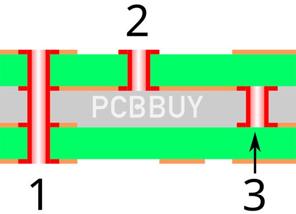
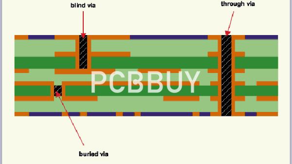
A blind via connects an outer layer to a specific inner layer without passing through the entire board. A buried via is located entirely between inner layers and is therefore invisible from the outside. The criteria for determining whether these two types of vias require resin plugging are not the same.
The main concern with buried vias arises before lamination. After drilling and plating, buried vias must go through subsequent lamination cycles. If the holes remain hollow, the prepreg may not provide sufficient resin flow to fill the cavities during lamination. This can create depressions above the via openings, directly affecting fine-line fabrication and impedance control. During vacuum-assisted lamination, unfilled buried vias may also trap localized pockets of gas, weakening interlayer bonding quality.
For this reason, in most multilayer PCB designs, buried vias must undergo resin plugging before lamination to ensure surface flatness and interlayer reliability. This is a prerequisite, not an optional process.
The decision for blind vias depends on whether they serve a soldering function. For an outer-layer blind via that is not located within a pad or beneath a high-density package, solder mask coverage may be sufficient from a basic solder mask and moisture protection perspective. However, once a blind via is located in a via-in-pad structure, or the dielectric layer above it is relatively thin and will undergo multiple lamination cycles, solder mask coverage alone is no longer sufficient.
In simple terms, the core issue for buried vias is that the holes must be completely filled before lamination. For blind vias, the key question is whether the via opening must support soldering and long-term environmental protection.
2. Lamination Flatness: An Unfilled Cavity Can Affect Every Subsequent Lamination Cycle
One defining characteristic of high-layer-count PCBs is that they undergo multiple lamination cycles.
In a second-order or higher-order HDI board, the inner-layer buried vias must first be resin-plugged and plated flat to create a smooth, copper-covered landing surface. The upper-layer laser-drilled blind vias can then be drilled down to this landing surface to establish vertical interconnections between layers.
If the buried vias are not filled and planarized, the prepreg may flow under high temperature and pressure during lamination, but the hollow vias provide no solid internal support. Lamination pressure can cause the dielectric layer and copper foil above the holes to collapse into the cavities, creating localized depressions at stacked-via locations.
The consequence is not simply an unattractive surface. The surface copper thickness in these areas may deviate from its design value, changing the parasitic characteristics of the via structure and introducing additional reflection loss for high-frequency signals at stacked-via transitions.
For HDI stacked-via structures, Lieban supports laser-drilled blind vias with a minimum diameter of 0.075 mm. The laser via-fill plating depth ranges from 0.05 mm to 0.15 mm, with a depth tolerance of ±15%.
However, this capability depends on the buried vias already having a flat, dense, and properly planarized surface. Without this prerequisite, there is no reliable reference surface against which via-fill depth tolerances can be controlled.
3. Electrical Continuity in Stacked Vias: The Laser-Drilled Via May Not Connect to the Buried Via at All
The electrical principle of a stacked-via structure is straightforward: the filled and planarized buried via in the lower layer provides a copper landing surface, and the laser-drilled blind via in the upper layer reaches this surface to form a continuous metallic connection.
If the buried via is not filled, the bottom of the laser-drilled via may expose a hollow cavity or a residual dielectric/air interface rather than a solid copper surface after passing through the dielectric layer.
The result is direct: a reliable metallic connection between the laser-drilled via and the buried via cannot be established. This may result in an open circuit or an unstable, intermittent connection with highly variable contact resistance.
Such defects can be particularly difficult to identify with conventional two-wire flying probe testing. Two-wire measurements typically operate at the ohm level and may have difficulty detecting small high-resistance connections or poor contact at the via bottom.
Lieban uses four-wire low-resistance testing in its continuity testing process, with a stated measurement capability in the range of 0.1 μΩ to 0.1 mΩ. This is intended to help identify via-bottom interconnection abnormalities that may escape conventional two-wire testing and only become apparent after the board is assembled.
However, one distinction must be made clear: four-wire testing is a screening measure. Resin plugging followed by copper plating and planarization is the prerequisite for preventing this risk from developing in the first place. Using inspection to compensate for a defect that could have been eliminated through proper structural design is not a sound manufacturing approach for high-reliability products.
4. Thermomechanical Reliability: Hollow Cavities Amplify CTE Mismatch
High-layer-count PCBs used in automotive electronics, industrial control, energy storage, and embodied robotics must withstand repeated temperature cycles.
Automotive electronics commonly experience temperature cycling between −40°C and 125°C, while energy storage and power applications may also involve continuous electrical operation and localized self-heating.
Resin, laminate materials, and copper foil have different coefficients of thermal expansion (CTE). A hollow buried via effectively leaves an unfilled cavity within the interlayer structure, where there is no material to provide continuous mechanical support or stress transfer. As a result, thermal stress cannot be distributed through a continuous material structure and instead becomes concentrated around the via walls and openings.
A typical progression of this stress concentration begins with microcracks at the interfaces between the via walls and the resin or base material. These cracks may then develop into plated copper fractures, interlayer delamination, or even board blistering during reflow soldering or field temperature cycling.
Multiple lamination cycles in advanced HDI structures further amplify this effect. The resin-plugged buried vias in high-order HDI boards must already withstand repeated high-temperature lamination cycles, making CTE matching a significant process challenge. Without resin plugging, the problem escalates from a material-matching challenge to a structural weak point.
For HDI products serving automotive electronics and industrial control applications, Lieban specifies a thermal shock reliability requirement of 288±5°C for 10 seconds, repeated three times, in its outgoing standards. This test is intended to expose weaknesses in via-wall bonding and interlayer interfaces—precisely the areas that can be compromised by hollow buried vias.
In applications involving long-term electrical bias, unfilled buried-via cavities may also create discontinuous interfaces between the via walls and dielectric layers. These interfaces can provide migration paths for moisture and ions, increasing the risk of CAF (conductive anodic filament) failures.
By filling the via cross-section with dense epoxy resin, resin plugging helps eliminate this pathway.
5. Signal Integrity: Stacked Vias Are Designed to Reduce Via Stubs, but Hollow Cavities Introduce New Discontinuities
One of the main advantages of blind and buried vias over through-holes is their ability to reduce via stubs and impedance discontinuities.
In high-frequency and high-speed signal paths, a via stub acts like an unterminated section of transmission line, potentially causing signal reflections and resonance. Because a blind via connects only the required layers, it does not create the same full-length residual stub found in a conventional through-hole via.
However, this advantage depends on every via transition along the stacked-via path being continuous, dense, and geometrically predictable.
If buried vias are not filled and planarized, the resulting risks of poor contact at the via bottom, lamination depressions, and copper thickness deviations can introduce additional parasitic capacitance variations and impedance discontinuities along the stacked-via path. This undermines the intended electrical behavior of the vertical interconnection.
Lieban supports multilevel impedance control for HDI stacked-via boards and uses TDR impedance testing for first-article inspection, in-process inspection, and final inspection.
There is one point that both procurement teams and engineers can easily overlook: impedance testing verifies the structure that has actually been manufactured. If the prerequisite buried-via filling process is missing or inadequate, the impedance report reflects the impedance of the defective structure, not the intended design.
Therefore, when reviewing an impedance report, it is also important to ask whether the buried vias in the corresponding stacked-via structure underwent controlled resin plugging and copper plating to achieve a planarized surface.
6. Vacuum Filling or Screen Printing: High-Layer-Count PCBs Leave Little Room for Compromise
The term “resin plugging” may look like a single process on a quotation, but screen-printing-based filling and vacuum filling have fundamentally different characteristics in terms of internal fill quality.
Screen-printing resin plugging uses an inclined-arm screen printer with an aluminum stencil. By increasing printing pressure, resin is forced into the holes. However, there is no active mechanism for removing the air inside the holes. As resin moves forward, the trapped air is pushed back, making bubbles and voids inherent process risks.
Industry comparisons indicate that conventional screen-printing resin plugging typically achieves a fill rate of approximately 95%–98%, with a bubble rate in the range of 5%–10%.
Vacuum resin plugging, by contrast, requires the entire board to undergo vacuum extraction in specialized equipment before a mechanical squeegee forces resin through the holes. The vacuum environment removes trapped air as a process variable. This method can achieve a fill rate of over 99%, with the bubble rate controlled to ≤1%.
For high-layer-count PCBs, this is not simply a difference between a slightly better process and a slightly worse one. It represents a difference in the nature of the risks involved.
Bubbles left inside holes by screen-printing resin plugging may expand under the high temperatures and pressures of subsequent lamination, creating microscopic separation between the via walls and the resin. During peak reflow temperatures, the residual gas can expand further, potentially lifting solder joints above the pads or creating additional stress concentration points.
After a high-layer-count PCB has gone through multiple lamination and assembly reflow cycles, the unit cost saved by using screen printing may eventually be offset by microsection failures, rework, additional screening, or batch-level customer complaints.
Lieban uses a vacuum-based resin plugging process. For buried-via applications, Japanese Sumitomo resin is used, with a stated fill completeness of over 98%. The objective is to eliminate the internal cavity before the board undergoes multiple lamination cycles.
For HDI stacked-via and via-in-pad structures, vacuum resin plugging is combined with surface copper plating and planarization to eliminate the risks associated with having open holes beneath solder pads.
Internal controls for via-mouth recess are applied according to hole diameter:
-
For holes with a diameter ≤0.4 mm: recess ≤15 μm.
-
For holes with a diameter >0.4 mm: recess ≤50 μm.
These two limits are not arbitrary. Smaller holes are more difficult to fill with a precisely controlled amount of resin. Although the absolute recess may be small, its relative impact on surface flatness at the via opening can be greater.
7. What Level of Resin Plugging Is Sufficient? Not Every Via Needs to Be Upgraded to Resin Plugging
From a procurement perspective, resin plugging adds several process steps, including via filling, grinding, and copper plating or capping. Both unit price and lead time are therefore higher than those of solder mask coverage alone.
The right selection strategy is not to assume that a more expensive process is always safer. Instead, resin plugging should be applied where the internal condition of a via genuinely affects subsequent manufacturing processes or long-term reliability.
Applications where resin plugging is essential
-
Via-in-pad structures: Particularly via-in-pad designs beneath BGA packages. If the holes are only covered with solder mask rather than filled, solder paste may be drawn into the holes along the via walls during reflow. This can create voids beneath solder balls, leading to insufficient solder joints or, in more severe cases, cracks during thermal cycling.
-
Buried vias between layers: If they are not filled before lamination, the risks of surface depressions and compromised interlayer bonding cannot be eliminated.
-
Buried vias in stacked-via structures: Resin plugging followed by copper plating and planarization is essential. Otherwise, the upper laser-drilled vias will not have a reliable copper landing surface.
-
Vias larger than 0.45 mm in diameter that require complete filling: Solder mask plugging alone is physically difficult to use to achieve consistent full-hole filling.
Applications where solder mask coverage remains a reasonable option
-
Signal vias outside BGA and solder-pad areas, with conventional hole diameters and no direct solder paste contact with the via openings during soldering.
-
Outer-layer blind vias that do not participate in subsequent lamination, provided their openings are outside soldering areas.
-
Large non-functional vias or mounting holes, where resin plugging is neither economical nor likely to provide a corresponding reliability benefit.
FAQ
Q1: Why is vacuum resin plugging significantly more expensive than screen-printing resin plugging, even though both are listed as “resin plugging” on a quotation?
The price difference is not primarily in the resin material itself. It comes from the ability to remove air trapped inside the holes and the resulting differences in process yield distribution.
Screen-printing resin plugging has a relatively low equipment barrier, but bubbles and voids are inherent risks of the process principle. Vacuum resin plugging requires a stable vacuum environment created by a secondary vacuum chamber, vacuum extraction system, and sealing structure. The equipment investment is therefore on a completely different scale.
More importantly, the unit cost saved through screen printing on high-layer-count PCBs may eventually be offset by hidden scrap, rework, or customer-side failures caused by residual gas inside the holes.
Vacuum filling is about achieving a narrower and more consistent yield distribution, not promising that every board will be perfect.
When quoting, Lieban evaluates the plugging method, hole diameter, and whether subsequent copper capping is required together, rather than simply writing “resin plugging” as a general note.
Q2: Can buried vias be left without resin plugging and filled by resin flowing from the prepreg during lamination?
For conventional buried vias that are not part of a stacked-via structure, increasing the number of prepreg plies can provide some compensation through additional resin flow.
However, this approach does not work for stacked-via structures. Stacked vias require a flat copper surface above the buried via that can support subsequent laser drilling and copper plating. Resin flow during lamination cannot provide reliably controlled surface flatness or copper surface continuity, nor can it eliminate the risk of cavity collapse during subsequent lamination cycles.
For HDI buried-via applications, Lieban uses vacuum resin plugging to address a requirement that must be met in stacked-via structures, rather than treating it as an area where a compromise is acceptable.
Q3: How can buyers determine whether a supplier's resin plugging for blind and buried vias has been properly completed?
Focus on three practical checkpoints.
First, define the requirements clearly during the DFM review. Do not simply specify “resin plugging.” State explicitly that buried vias in stacked-via structures must undergo resin plugging followed by copper plating and planarization, with the finished surface meeting the requirements for subsequent laser drilling and copper coverage.
Second, request microsection data. Pay particular attention to whether the filled vias contain bubbles or voids and whether the resin is tightly bonded to the via walls.
X-ray inspection can be used as an in-process screening method, but metallographic microsection analysis is the actual basis for determining whether the internal fill is complete.
Lieban's inspection process includes X-ray equipment for examining inner-layer structures and lamination registration in high-layer-count PCBs. Metallographic microscopes are also used for cross-sectional confirmation of resin fill completeness and void conditions.
For automotive and industrial control orders, microsection analysis is a required part of first-article approval and periodic reliability sampling, not simply an abnormality investigation performed after a problem occurs.
Third, verify the required via copper thickness grade. Lieban offers multiple via copper thickness grades, including 18 μm, 20 μm, 25 μm, 30 μm, and 35 μm. For automotive, industrial control, and power electronics products, it is advisable to define the via copper requirements together with the resin plugging process during engineering review rather than confirming them separately.
Q4: What level of surface recess is acceptable after resin plugging for via-in-pad structures?
In industry practice, the recess for ordinary signal vias is typically required to be ≤15 μm. The requirements for via-in-pad structures are stricter because they directly consume the coplanarity margin available for SMT placement.
For Class 3 products, the recess limit for filled vias referenced by IPC-4761 is in the range of ≤5 μm, while Class 2 requirements are relatively less stringent.
Lieban applies internal controls based on hole diameter:
-
For holes with a diameter ≤0.4 mm: recess ≤15 μm.
-
For holes with a diameter >0.4 mm: recess ≤50 μm.
One important point needs to be clarified: if copper capping is performed after resin plugging, the reference surface for measuring recess should be the finished pad surface after copper capping, not the resin surface after grinding.
A typical copper cap thickness requirement is no less than 25 μm. Its integrity directly affects whether the pad can maintain its structural stability during thermal cycling without collapsing due to a cavity beneath the resin.
Q5: What reliability tests should be performed before shipping high-layer-count PCBs after resin plugging?
Passing a static microsection inspection does not necessarily mean the board will remain reliable after reflow soldering and thermal cycling.
Lieban's outgoing standards include physical tests such as solderability testing, with a wetting area of >95% and complete wetting of plated through-holes, as well as thermal shock testing at 288±5°C for 10 seconds, repeated three times.
For HDI products used in automotive electronics and industrial control applications, this thermal shock condition is consistent with the thermal reliability validation approach for vacuum resin-plugged structures. It can help cross-verify the combined heat resistance of the resin plugging and plated copper.
For automotive electronics applications, Lieban has obtained IATF 16949 quality management system certification. Its process selection is guided by long-term insulation reliability and thermomechanical stability, rather than treating successful electrical testing as the final acceptance criterion.
Conclusion
Resin plugging for blind and buried vias in high-layer-count PCBs essentially serves one purpose: eliminating the internal cavity as an uncontrolled variable within the interlayer structure.
Lamination requires a flat landing surface. Stacked vias require continuous copper connections. Thermal cycling requires continuous material structures without stress concentration points. Signal integrity requires geometrically predictable via transitions. Long-term insulation reliability requires blocking pathways through which moisture and ions can migrate along interfaces.
All these requirements point to the same manufacturing process, but they do not necessarily demand the same level of via filling.
For design engineers, the key is to distinguish between vias that must undergo resin plugging and those for which solder mask coverage is sufficient during the design stage. Requirements for filling and planarizing buried vias in stacked-via structures should be explicitly included in the DFM documentation rather than left in general notes for the supplier to interpret.
For procurement teams, the key is to evaluate the price difference between vacuum filling and screen-printing filling within the context of total cost. On a high-layer-count PCB, the cost of an undetected cavity that emerges during lamination, SMT assembly, or customer-side operation is usually far greater than the unit price saved by choosing a less controlled process.
Lieban's manufacturing configuration for high-layer-count and HDI PCBs—including vacuum resin plugging, four-wire low-resistance testing, X-ray and metallographic microsection inspection, multiple via copper thickness options from 18 μm to 35 μm, and 288±5°C thermal shock validation for automotive and industrial control products—reflects a consistent engineering principle:
The reliability of blind and buried vias is not established by what is written in the outgoing inspection report. It is built through the actual manufacturing process: resin filling, vacuum extraction, curing, grinding, and layer-by-layer verification.
Industry Category