HDI Multilayer PCB Manufacturing Capabilities Solutions
By:PCBBUY 06/18/2025 15:00
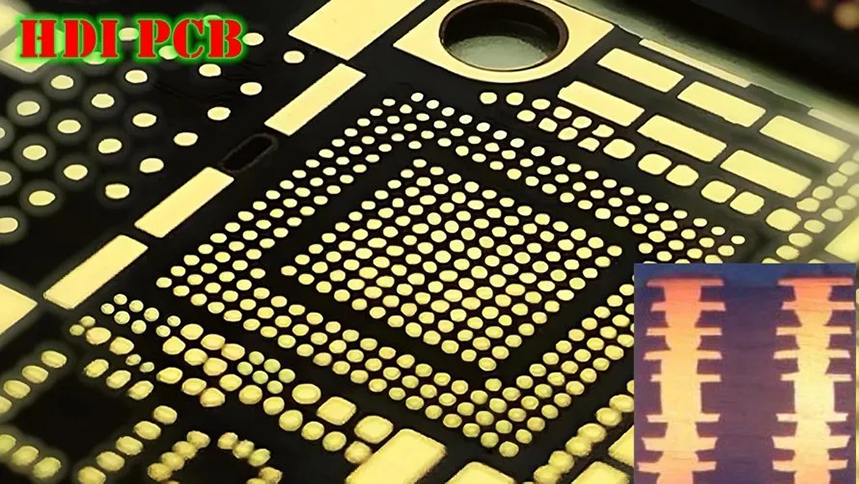
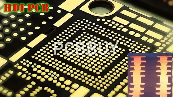
As the demand for high-density interconnect (HDI) multilayer PCBs continues to surge across industries like automotive electronics, telecommunications, and IoT devices, choosing a reliable manufacturer with proven capabilities becomes crucial. At PCBBUY, we specialize in delivering HDI multilayer PCB solutions that meet stringent design and performance requirements. In this article, we provide an in-depth look at our HDI manufacturing capabilities based on our internal process standards and how they translate to high-quality PCB production.
Materials for HDI Multilayer PCB
TG135–TG170 FR-4 and Halogen-Free Options
At PCBBUY, we use FR-4 as the standard material for HDI multilayer PCB fabrication, with support for TG135 to TG170 range to meet different thermal and mechanical performance needs. Additionally, halogen-free and CTI-rated materials can be customized based on customer specifications for higher safety and environmental standards.
Layer Count Flexibility in HDI Multilayer PCB Stackups
From 4-Layer to 10-Layer and Beyond
Our manufacturing supports:
-
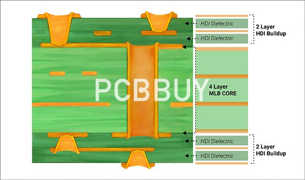
1st Order HDI: 4 to 10 layers
-
2nd Stage HDI: 6 to 10 layers
This flexibility allows PCBBUY to deliver complex HDI multilayer PCB stack-ups that are suitable for both consumer-grade and industrial-grade electronics.
Construction Types for HDI Multilayer PCB
Sequential Lamination with Buried and Blind Vias
We support a wide variety of HDI constructions, including:
-
1st order: 1+N+1, 1+1+N+1+1 (with buried vias ≤ 0.3 mm)
-
2nd order: 2+N+2, 1+2+N+2+1
We typically prefer internal mechanical vias for enhanced structural integrity, but where design limits apply, we offer electroplating via filling processes as an alternative.
HDI Multilayer PCB High Precision Trace Width and Spacing
Minimum 2/2 mil for Fine-Line Capability
Our HDI multilayer PCB lines are manufactured with minimum 2/2 mil trace width/spacing, enabling ultra-compact routing ideal for mobile devices, wearables, and HDI applications.
HDI Multilayer PCB Advanced Blind Via Capabilities
Laser and Mechanical Blind Via Support
We offer both:
-
Mechanical blind holes: ≥ 0.15 mm
-
Laser blind holes: ≥ 0.075 mm
These capabilities allow for more flexible routing between layers, reducing layer count and saving PCB real estate.
HDI Multilayer PCB Minimum Drilled Hole Size
Unilateral Hole Size ≥ 3 mil
To support high-density BGA components and fine-pitch designs, PCBBUY guarantees drill accuracy with minimum unilateral hole size of 3 mil, enabling us to manufacture intricate via structures with reliable plating quality.
HDI Multilayer PCB Hole Copper Thickness Standards
Ensuring Structural and Electrical Reliability
Our plating specifications for via copper include:
-
Mechanical hole (no laser): copper thickness > 18 μm
-
Laser blind holes: copper thickness > 13 μm
This ensures sufficient current-carrying capacity and long-term reliability in multilayer boards.
HDI Multilayer PCB Via Electroplating Capabilities
Electroplated Copper Filled Vias for HDI Multilayer PCBs
For filled via applications:
-
Electroplating depth: 0.05 mm – 0.1 mm
-
Depth tolerance: ±15%
We use high-precision electroplating techniques to ensure the surface of the hole is fully metalized, providing robust interlayer connections and minimizing signal distortion.
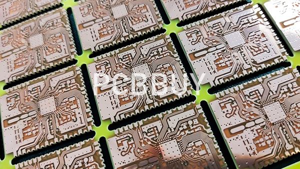
HDI Multilayer PCB Manufacturing Process Optimization at PCBBUY
Process Review and Customization Available
All specifications in our HDI multilayer PCB workflow can be reviewed and tailored:
-
Customized material stack-ups
-
Application-specific blind/buried via combinations
-
Electroplating strategies based on current load and thermal demands
Our engineers collaborate closely with clients during the DFM (Design for Manufacturability) phase to optimize performance, cost, and production yield.
Why Choose PCBBUY for Your HDI Multilayer PCB Projects?
With decades of PCB manufacturing experience and strict adherence to IPC standards, PCBBUY offers one-stop HDI multilayer PCB fabrication with a focus on quality, reliability, and flexibility. Whether you're prototyping or scaling to mass production, our advanced capability matrix ensures that your complex design can be manufactured with confidence.
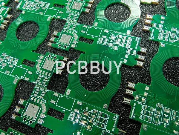
HDI Multilayer PCBs AQ
To help you better understand the unique characteristics and advantages of HDI multilayer PCBs, here are answers to some of the most frequently asked questions.
What Is the Difference Between HDI Multilayer PCBs and Standard PCBs?
HDI multilayer PCBs (High-Density Interconnect) are distinguished from traditional PCBs by their higher interconnection density, finer lines/spaces, smaller vias, and thinner materials.
Here's a comparison:
|
Feature |
Standard Multilayer PCB |
HDI Multilayer PCB |
|
Trace Width/Spacing |
≥ 4/4 mil |
≥ 2/2 mil |
|
Via Type |
Through-hole |
Blind/Buried/Laser via |
|
Layer Interconnect |
Basic stack-ups |
Advanced sequential lamination (1+N+1, 2+N+2) |
|
Component Density |
Low to moderate |
Very high |
|
Signal Integrity |
Standard |
Optimized for high-speed signals |
|
Cost |
Lower |
Higher due to complexity |
HDI multilayer boards are especially valuable in space-constrained, signal-sensitive, and high-performance electronic designs—such as smartphones, automotive control units, and aerospace equipment.
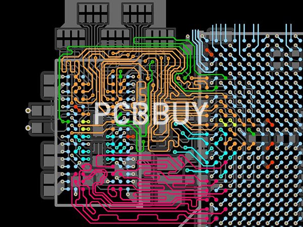
Why Are HDI Multilayer PCBs More Expensive?
The cost of manufacturing HDI multilayer PCBs is higher for several key reasons:
-
Advanced Fabrication Equipment: Laser drilling, via filling, and sequential lamination require specialized, high-precision machinery.
-
Increased Process Steps: HDI PCBs may involve multiple lamination cycles and more intricate quality checks.
-
Material Requirements: High TG materials, halogen-free options, or low Dk/Df substrates add to raw material costs.
-
Yield Challenges: Due to the tight tolerances, more stringent process controls are needed to ensure acceptable yields.
While the cost is higher than conventional PCBs, the performance gains and miniaturization benefits often justify the investment in HDI technology.
What Testing and Certifications Are Offered?
To guarantee the reliability and performance of HDI multilayer PCBs, PCBBUY provides multiple in-house and third-party testing options:
|
Testing Method |
Description |
|
Flying Probe Test |
Non-contact, electrical continuity and isolation test for prototypes or small batches |
|
X-ray Inspection |
Used to verify BGA soldering, internal via structures, and detect hidden defects |
|
Impedance Control Measurement |
Ensures critical signals meet high-speed requirements |
|
Microsection Analysis |
Cross-sectional inspection of vias and multilayer structures |
|
Solderability Test |
Verifies PCB surface finishes can be reliably soldered |
|
AOI (Automated Optical Inspection) |
High-speed visual inspection for surface defects |
We also comply with IPC Class 2 or Class 3 standards, RoHS, and REACH directives to support international markets.
What Is the Fastest Prototype Turnaround for HDI Multilayer PCBs?
At PCBBUY, we understand the importance of speed in product development. Our expedited services can deliver:
-
HDI Multilayer PCB prototypes in as fast as 5 working days
-
Standard lead time for complex HDI stack-ups: 7–10 working days
-
Mass production orders: Depending on layer count and complexity, typically 10–15 working days
Contact our service team to request expedited processing or for support on urgent projects.
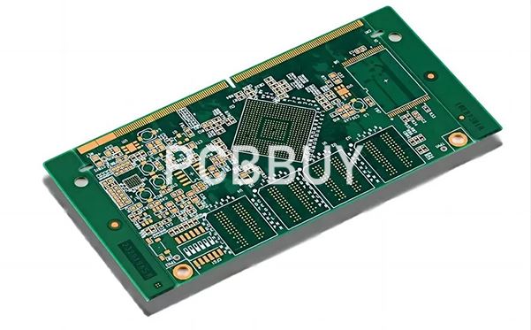
Conclusion
PCBBUY’s HDI multilayer PCB manufacturing capabilities combine precision, customization, and advanced process controls. From material selection to blind via plating, every step is optimized for high-performance applications. Trust PCBBUY to deliver your next generation of HDI PCBs with industry-leading consistency and service.
From understanding why HDI multilayer PCBs differ from traditional PCBs, to learning about testing options and turnaround times, it's clear that PCBBUY is equipped to handle complex HDI requirements with both speed and precision.
Whether you’re working on high-speed data transmission, RF designs, or ultra-compact modules, our expert engineering team is ready to bring your vision to life.
Industry Category


