How to Choose a PCB Manufacturer: Key Equipment and Manufacturing Capabilities to Evaluate
By:PCBBUY 11/13/2026 14:49

When choosing a PCB manufacturer, it is easy to focus on the numbers in a capability chart. Maximum layer count, minimum trace width, smallest drill size, and advertised production lead time all look like useful indicators. However, these figures only show what a factory may be able to produce under certain conditions. They do not necessarily demonstrate that the same results can be maintained consistently in volume production.
After more than 20 years in PCB manufacturing, I have seen two recurring mistakes in supplier selection. In one case, procurement teams choose a factory mainly because its equipment list shows more impressive specifications. In another, buyers focus almost entirely on unit price and discover quality or process-control issues only after the boards arrive. A via barrel may have insufficient copper at a localized thin area. An impedance coupon may never have been measured. A prepreg combination may have been changed between the prototype build and mass production without adequate approval.
Equipment defines the physical limits of a PCB production line, but it does not tell the whole story. The more important question is whether a manufacturer can repeatedly hold the required process parameters across production lots, not simply whether it can produce one acceptable sample.
This distinction matters even more in applications such as automotive electronics, industrial control, power electronics, energy storage, new energy systems, and embodied robotics, where field failures can lead to costly downtime, safety concerns, and difficult product recalls.
The following five areas provide a practical framework for engineers and procurement teams evaluating a PCB manufacturing partner. Each section connects the equipment and process controls to the manufacturing capabilities stated by PCBBUY

1. Certifications and Quality Systems: Check the Scope, Not Just the Certificates
ISO 9001 is an important foundation for a quality management system, but it should not be the only criterion when evaluating a PCB supplier. For industry-specific applications, the scope and actual implementation of additional quality systems can make a significant difference.
For automotive electronics, IATF 16949 is particularly relevant. Its value is not simply the certificate displayed at a factory entrance. Buyers should understand whether core quality tools such as APQP, PPAP, FMEA, SPC, and MSA are integrated into the actual workflow, from contract review and process planning to production monitoring and final inspection. These methods help manufacturers identify process risks, establish control plans, monitor variation, and maintain production consistency.
UL recognition is also important when PCB materials or finished boards are subject to safety requirements. For power supplies and other end products requiring electrical safety evaluation, buyers should confirm that the relevant board construction, materials, and manufacturing site fall within the applicable UL requirements. RoHS and REACH should be treated as regulatory compliance requirements rather than interchangeable quality-system certifications.
When auditing a supplier, ask whether the certificates cover only the company's headquarters or also the specific production facilities that will manufacture your orders. It is equally important to review the scope of the latest external audit, outstanding nonconformities, and corrective-action records. A certificate alone does not prove that every production line operates under the same controlled conditions.
PCBBUY states that it holds ISO 9001 and IATF 16949 quality management system certifications, along with UL product recognition and RoHS and REACH compliance. Its two company-operated production facilities in Zhuhai are stated to be within the quality-system coverage. These capabilities are relevant to automotive electronics, industrial control, power equipment, energy storage, new energy systems, and embodied robotics. For a specific project, however, buyers should still verify the certificate numbers, validity periods, product scope, and site coverage.
2. Imaging and Circuit Patterning: Why LDI Must Work Together with Etching Control
Laser Direct Imaging (LDI) is often treated as an upgraded exposure machine, but its real value is in how it changes the pattern-transfer process.
Traditional phototool-based exposure relies on film artwork. Dimensional changes in the film can be affected by temperature, humidity, and handling, introducing additional registration variation. LDI eliminates the physical phototool from the imaging step and transfers the circuit pattern directly onto the photoresist using a laser. It can also compensate for measured panel scaling, helping improve layer-to-layer registration and pattern consistency.
This becomes particularly important for thick boards, large-format panels, and high-layer-count PCBs. As board thickness and layer count increase, maintaining registration becomes more challenging. A small amount of dimensional variation can affect annular rings, clearances, and the reliability of connections between layers. In these applications, LDI is not simply a way to produce finer traces; it is part of a broader strategy for controlling pattern registration.
However, imaging accuracy is only one part of circuit quality. Etching control determines whether the transferred pattern can be reproduced with the intended conductor width and spacing.
During conventional spray etching, the exchange of fresh etchant with reacted chemistry at the copper surface can become less effective under certain process conditions. This may contribute to uneven etching, conductor-width variation, and irregular trace profiles. These effects become more difficult to manage when heavy copper and fine-line features are present on the same design.
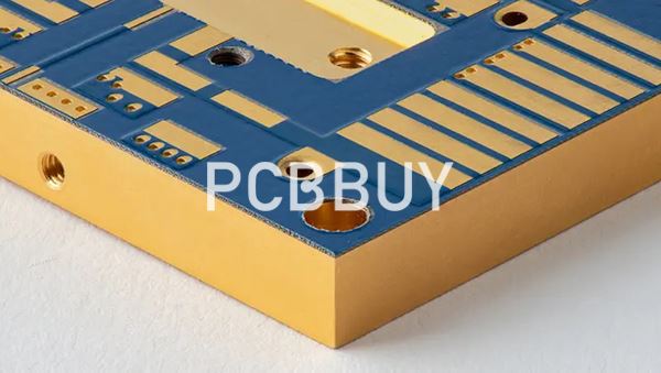
PCBBUY uses a DES (Developing, Etching, and Stripping) production line equipped with vacuum-assisted precision etching for heavy copper processing. The vacuum-assisted section is designed to remove spent etchant from the copper surface and improve the exchange of fresh chemistry during etching. This helps address process challenges associated with heavy copper and circuit-pattern consistency.
The manufacturer's stated LDI registration capability is approximately ±10 μm. Combined with controlled etching, this forms a process chain that connects imaging accuracy with the final conductor geometry. When evaluating a supplier, engineers should ask how registration is measured, how etching compensation is applied, and whether trace-width results are monitored across the production panel rather than checked at only one location.
3. Drilling and Plating: What Does an 18 μm Via Copper Requirement Actually Mean?
Via-wall copper thickness is one of the most important factors to review when selecting a PCB manufacturer, particularly for high-reliability products. It is also an area where capability figures can be misunderstood.
A supplier may state that its via copper thickness is 18 μm and describe this as an IPC Class 2 requirement. However, a single thickness figure is incomplete unless the measurement basis is clear. Engineers need to know whether the value refers to an average, a minimum thin-area measurement, or an internal process-control target.
For rigid printed boards, IPC-6012F distinguishes between average hole-wall copper thickness and thin-area requirements. In the applicable through-hole plating requirements, Class 2 specifies an average copper thickness of 20 μm and a thin-area minimum of 18 μm. Class 3 specifies an average of 25 μm and a thin-area minimum of 20 μm. The applicable requirements should always be checked against the board type, construction, drawing notes, and contractually specified revision.
This is why asking only whether a factory can achieve 18 μm is not enough. Buyers should ask how the manufacturer evaluates the result, where the measurement locations are taken, how many microsections are inspected, and what internal process-control limits are used. A single passing measurement does not demonstrate uniform plating throughout a production lot.
PCBBUY states that its default internal control target for via-wall copper is above 18 μm at individual measurement points. It also offers several selectable copper-thickness levels: 18 μm, 20 μm, 25 μm, 30 μm, and 35 μm. For boards used in high-current, high-voltage, or frequent pulse-load applications, the manufacturer recommends considering a 25 μm via copper requirement at the order-review stage. The actual specification should be agreed upon in the fabrication notes and confirmed through the relevant inspection records.
Deep-Hole Plating and Copper Uniformity
The performance of a plating line becomes particularly important when manufacturing boards with high aspect ratios. A deep hole is more difficult to plate uniformly because solution exchange and current distribution become increasingly challenging as the hole depth increases relative to its diameter.
PCBBUY lists a 13:1 aspect-ratio capability for its automatic vertical electroless copper and vertical electroplating lines. This capability is relevant to designs requiring deep-hole interconnections, but the achievable result still depends on the finished board thickness, drill diameter, hole geometry, copper requirement, and production conditions.
The manufacturer also describes several features of its plating process. An air-source heat pump central hot-water circulation system is used in place of conventional electric heating elements immersed in the plating solution. This arrangement is intended to reduce localized heating and the risk of contamination associated with direct-contact heating elements. Customized anodes, ultrasonic assistance, and side-spray configurations are also used to support solution circulation and plating distribution.
PCBBUY states a copper-thickness uniformity figure of at least 97%. Before comparing this figure with another supplier's data, ask for its exact definition, calculation method, sampling locations, and supporting microsection results. A percentage without a defined measurement method is difficult to use as a meaningful quality benchmark.
The manufacturer also specifies the use of microcrystalline phosphorized copper balls as an anode material rather than reclaimed copper pieces. Anode material quality can influence the stability and cleanliness of the plating bath, but the finished via-wall copper quality must still be verified through process monitoring and appropriate inspection.
For high-aspect-ratio boards, the most useful supplier evidence is not just a maximum aspect-ratio claim. It is a combination of representative production records, cross-section results, plating-thickness distribution, and documented process limits.

4. Resin Plugging and Interlayer Reliability: Why Vacuum Filling Matters
Resin plugging is increasingly important in multilayer PCB designs, particularly when via-in-pad structures or other designs requiring filled holes are used. The choice of filling process can affect void formation, surface flatness, and subsequent processing.
Conventional screen-printing methods use mechanical pressure to push resin into the holes. Depending on the hole geometry, resin properties, printing conditions, and process setup, air may remain trapped inside the hole. This can lead to incomplete filling or internal voids. Vacuum-assisted resin filling uses reduced pressure to help remove trapped air before or during filling, improving the opportunity for resin to enter the hole more completely.
The difference should not be judged by the process name alone. Published comparisons sometimes quote fill rates of 95–98% for conventional screen printing and above 99% for vacuum filling, with corresponding differences in void rates. These figures are process-dependent and should not be treated as universal industry benchmarks. The actual result depends on resin viscosity, hole diameter, aspect ratio, vacuum conditions, printing parameters, curing, and the method used to define a void or filling percentage.
Why does this matter? Residual voids or insufficient filling may become more problematic during soldering and thermal cycling. Trapped gas can expand at elevated temperatures, while incomplete filling and uneven resin distribution may contribute to local stress or surface defects. Depending on the board construction and downstream assembly process, these conditions can increase the risk of soldering issues or reliability failures.
PCBBUY uses a vacuum resin-filling process and specifies Japanese Sumitomo resin for this application. The manufacturer states that resin fill completeness is controlled above 98%. For holes with a diameter of 0.4 mm or less, the specified surface depression is no more than 15 μm. For holes larger than 0.4 mm, the specified depression is no more than 50 μm.
These figures are more useful when supported by actual cross-section images and inspection criteria. Buyers comparing two suppliers with different resin-plugging prices should ask whether the process uses vacuum equipment, what resin system is applied, how fill completeness and surface depression are measured, and whether the inspection results are recorded for each production lot.
The cost difference is not simply the price of the resin. It may also reflect the filling equipment, process controls, inspection frequency, and yield management required to achieve a more consistent result.
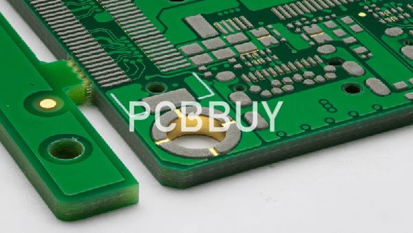
5. Inspection and Acceptance Standards: Four-Wire Testing and IPC Requirements
A PCB can pass a conventional electrical continuity test and still contain defects that deserve further investigation. This is particularly relevant to plated through-holes, where localized copper-thickness variation or a weak interconnection may not produce an open circuit during a basic electrical test.
A standard two-wire resistance measurement includes the resistance of the test leads and contact interfaces. This is generally adequate for ordinary continuity testing, but it can limit measurement accuracy when very low resistance values need to be evaluated.
Four-wire Kelvin measurement uses separate current and voltage-sensing connections. Because the voltage is measured independently of the current-carrying leads, the effect of lead and contact resistance can be reduced. This makes the method more suitable for detecting small resistance differences in low-resistance PCB circuits and interconnections.
For PCB inspection, four-wire testing can help identify abnormal resistance changes associated with via or plated-through-hole integrity. It should not, however, be described as a direct measurement of hole-wall copper thickness. Resistance is influenced by the entire measured current path, including conductor geometry, material properties, temperature, and probe placement. Microsection analysis remains an important method for directly examining plated-hole copper thickness and internal structural conditions.
PCBBUY has a Han's Laser automated four-wire low-resistance testing machine and includes this method in its inspection capability for relevant applications. It is intended to help identify electrical abnormalities that may not be detected by conventional continuity testing. For automotive, military, and other high-reliability applications, buyers should confirm whether four-wire testing is available for the specific design, which nets or test structures are measured, and what resistance limits determine acceptance.
Impedance Testing Must Include Physical Measurement
Impedance control is another area where buyers should distinguish theoretical calculation from production verification.
A manufacturer can calculate a target impedance from the proposed stackup, dielectric thickness, copper thickness, and trace geometry. This calculation is necessary, but it does not prove that the finished PCB meets the target. Actual impedance is affected by material properties, lamination variation, etching, and the final conductor geometry.
A more complete process uses impedance coupons designed into the production panel. The manufacturer measures these coupons with an impedance analyzer and compares the measured values with the specified target and tolerance. First-article, in-process, and final inspection records provide a more useful picture of process stability than a calculation report alone.
PCBBUY states that it performs theoretical impedance simulation based on customer design data and uses impedance coupons for physical measurement during production. Its stated measurement ranges are 10–150 Ω for single-ended impedance and 20–200 Ω for differential impedance, with a stated measurement accuracy of ±1%. Impedance reports can be provided when required.
When reviewing these figures, buyers should distinguish instrument accuracy from the acceptance tolerance of the finished board. They should also confirm the test method, coupon design, reference impedance, measurement frequency, and reporting format. For high-speed and high-frequency designs, these details are essential to determining whether the measured result is meaningful for the actual application.

Specify the Applicable IPC Class and Revision
Another common source of disagreement is an undefined IPC acceptance requirement. If the purchase order or fabrication drawing does not specify the required class and applicable revision, the manufacturer may apply its default acceptance criteria. A buyer may assume that a more stringent requirement applies, while the factory may have quoted and manufactured the board to a different class.
IPC-A-600 provides visual guidance for interpreting acceptable and nonconforming conditions on printed boards. IPC-6012 defines qualification and performance requirements for rigid printed boards. These documents serve related but different purposes, so they should not be treated as interchangeable.
PCBBUY's published acceptance information lists IPC-A-600J Class 2 and Class 3 as selectable inspection levels. However, IPC-A-600J is an older revision. Buyers preparing new orders should confirm the applicable current revision and align it with the corresponding performance specification, customer drawing, and purchase-order requirements. The current IPC-A-600 revision is M (2025), while IPC-6012 revision F was published in 2023.
The manufacturer also provides different stated capability ranges for different material systems. For the listed Kingboard/Guoji material combinations, the stated average via copper thickness is 18–20 μm; for Kingboard/Shengyi combinations, it is 20–25 μm. The stated board outline tolerances are ±0.13 mm and ±0.10 mm, respectively, with ±0.05 mm available by request. The corresponding stated board warpage limits are no more than 0.75% and 0.5%.
These figures should be reviewed as manufacturer-specific process capabilities, not as universal IPC acceptance limits. Buyers should confirm the exact laminate grade, stackup, copper measurement definition, outline measurement method, warpage calculation, and agreed acceptance class before placing an order.
6. How to Evaluate a PCB Manufacturer Beyond Its Equipment List
The following table summarizes the evidence worth requesting during supplier qualification. A capability figure is useful, but it becomes much more meaningful when supported by a defined measurement method and production records.
| Manufacturing Area | What to Evaluate | Evidence to Request |
|---|---|---|
| Quality management | ISO 9001, IATF 16949, UL recognition, and site coverage | Valid certificates, audit scope, corrective-action records |
| Imaging and circuit patterning | LDI registration accuracy and trace-width consistency | Registration data, trace-width inspection results, process-control records |
| Etching | Heavy-copper etching consistency and conductor profile | Cross-sections, trace-width measurements, etching-control records |
| Drilling and plating | Aspect ratio, via-wall copper thickness, and plating uniformity | Microsection reports, copper-thickness data, plating process limits |
| Resin plugging | Fill completeness, void control, and surface depression | Cross-section images, resin specifications, inspection criteria |
| Electrical testing | Continuity, four-wire low-resistance testing, and impedance measurement | Test coverage, resistance limits, impedance reports |
| Final acceptance | Applicable IPC class and revision, outline tolerance, and warpage | Approved fabrication notes, inspection records, certificate of conformance |
The key is to evaluate the relationship between equipment, process parameters, and outgoing inspection. A factory may own an advanced imaging machine, but that does not automatically guarantee consistent trace geometry. A plating line may be rated for a high aspect ratio, but the actual result still depends on the board construction and plating conditions. A four-wire tester may be available, but its value depends on whether the relevant circuits are included in the test plan.
A qualified supplier should be able to explain not only what its equipment can do, but also how the process is controlled, how deviations are detected, and what evidence is retained for each production lot.
FAQ
Is 18 μm via copper thickness enough for IPC Class 2?
Not as a standalone specification. Under the applicable IPC-6012F through-hole plating requirements, Class 2 specifies an average copper thickness of 20 μm and a thin-area minimum of 18 μm. The two values describe different measurement criteria. Buyers should therefore confirm whether a supplier's quoted 18 μm refers to a thin-area minimum, an internal process target, or an average measurement.
PCBBUY states that its internal control target is above 18 μm at individual measurement points and offers selectable via copper thickness levels of 18 μm, 20 μm, 25 μm, 30 μm, and 35 μm. For demanding applications, the required copper level and acceptance criteria should be agreed upon before production.
How can procurement teams compare different resin-plugging prices?
The first step is to compare the actual process and inspection requirements rather than the resin material alone. Ask whether the supplier uses vacuum-assisted filling, which resin system is specified, and how it controls fill completeness, internal voids, and surface depression.
PCBBUY states that its vacuum resin-plugging process uses Sumitomo resin, with fill completeness controlled above 98%. Its stated surface-depression limits are 15 μm or less for holes no larger than 0.4 mm and 50 μm or less for holes larger than 0.4 mm. Requesting cross-section evidence and lot-level inspection records will help determine whether the quoted process capability is relevant to your board design.
Why does one PCB manufacturer charge extra for impedance testing while another does not?
The difference may come down to whether the quoted service includes only theoretical impedance calculation or actual measurement of production coupons. A calculation based on the stackup is useful during design review, but it does not verify the finished board.
Physical impedance testing requires coupon design, production-panel space, test equipment, measurement time, and inspection records. PCBBUY states that it uses impedance coupons and an impedance analyzer for production measurements, with a stated range of 10–150 Ω for single-ended impedance and 20–200 Ω for differential impedance. Buyers should confirm whether the quoted price includes physical measurement and a formal report.
Are a minimum trace width of 2 mil and a minimum drill size of 0.1 mm enough to qualify a PCB manufacturer?
No. These figures describe individual manufacturing limits, not necessarily the supplier's standard production capability or its ability to maintain yield at volume. A 2/2 mil line-and-space capability, for example, should be evaluated together with copper thickness, etching compensation, panel size, material, and the required yield.
The same applies to a 0.1 mm drill. The achievable result depends on board thickness, aspect ratio, hole quality, plating requirements, and the production process. PCBBUY states a standard trace width and spacing capability of 3/3 mil, supported by LDI imaging and precision etching. Its vertical electroless copper and electroplating lines are specified for an aspect ratio of up to 13:1. Buyers should request representative production data for a construction similar to their own design.
Conclusion
Choosing a PCB manufacturer requires more than comparing equipment lists, maximum layer counts, or minimum feature sizes. Those figures describe the potential limits of a production line. They do not prove that the manufacturer can maintain the required quality across repeated production lots.
For automotive electronics, industrial control, power electronics, energy storage, new energy systems, and embodied robotics, the more useful evaluation focuses on how each manufacturing process is controlled and verified. Quality-system coverage establishes the management framework. LDI and precision etching help maintain circuit-pattern consistency. Deep-hole plating and clearly defined via copper requirements support interconnection reliability. Vacuum resin plugging helps control filling quality. Four-wire low-resistance testing and physical impedance measurement provide additional evidence beyond conventional continuity checks.
PCBBUY's stated capabilities include ISO 9001 and IATF 16949 quality systems, LDI registration control of approximately ±10 μm, a 13:1 plating aspect-ratio capability, selectable via copper thickness levels, vacuum resin plugging, automated four-wire low-resistance testing, and production impedance measurement.
For any supplier, including PCBBUY, the most important step is to connect each capability claim to an agreed specification, a defined inspection method, and traceable production evidence. Equipment sets the manufacturing boundary. Process controls determine repeatability. Inspection records show whether the finished boards meet the requirements. When all three are aligned, buyers can make a much more informed decision about a PCB manufacturer's suitability for demanding production work.
Industry Category