PCB inspection
By:PCBBUY 04/30/2021 18:10

No matter what kind of printed circuit boards you’re building or what type of device they’re being used for, your PCBs need to function correctly. These boards are the keys to the performance of many products, and malfunctions can have serious consequences.
Inspecting PCBs throughout the design, PCB manufacturing and PCB assembly processes is crucial to assuring that your product meets quality standards and operates as expected. Today, PCBs are complex. While this complexity makes room for lots of new capabilities, it also creates more chances for failures. As PCBs have gotten more advanced, so have the inspection techniques and technologies used to ensure their quality.
You can choose from various methods of PCB inspection. The right technique to use depends on the PCB type, the current step in the production process and the faults for which you want to test. Creating an adequate inspection and testing plan is crucial for ensuring a high-quality product.
Why do PCB need inspections?
Inspection is a critical step in any PCB production process. It can help you to catch defects so that you can correct them and improve your overall operation.
Inspecting your PCBs can uncover any defects that may have occurred during manufacturing or assembly. It can also help to reveal any design flaws that may exist. Checking PCBs after each phase of the process enables you to catch flaws before moving on to the next stage, which can save you from wasting further time and money on a defective product. It can also help you catch one-off defects that affect one or several PCBs. This process helps to ensure consistent quality among your boards and final products.
Without a proper PCB inspection procedure in place, flawed boards may make it into the hands of customers. If a customer receives a faulty product, your company may lose money through warranty payments or returns. The customer will also lose some of the trust they had in your company, and your reputation will suffer. This situation can result in missed opportunities if that customer takes their business elsewhere.
How to do PCB inspection?
What is Manual Visual Inspection?
The simplest form of PCB inspection is manual visual inspection (MVI). To perform this type of test, a worker looks over the board either with the naked eye or through magnification. They’ll compare the board to the design documents to ensure that all specifications were met. They’ll also look for common defaults. The type of defects they look for vary depending on the kind of board they’re checking and the components on it.
Ensure that the board’s thickness is correct, and check for surface roughness and warpage. Check the dimensions of the assembly match the specification. Inspect the integrity and clearness of conductive patterns, and check for solder bridging, open circuits, burrs and voids. Check the surface quality, then look for the existence of pits, dents, scratches, pinholes and other defects on printing traces and pads. Verify that all vias are in the correct positions. Inspect the firmness, roughness and brightness of pad plating, and check for any bulge defects. Assess coating quality.
It’s simplicity and low-cost. You don’t need any specialized equipment except potentially for magnification. You can also conduct these inspections very quickly.
What is Automated Optical Inspection?
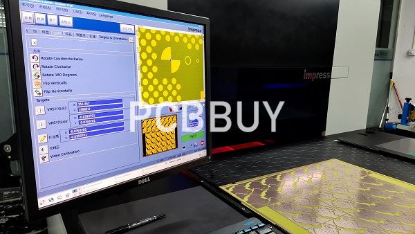
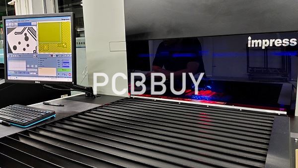
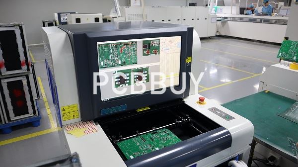
You can also use a PCB inspection machine to conduct a visual inspection. This method is called automated optical inspection (AOI).
An AOI system conducts an inspection using several light sources and one or more still or video cameras. The light sources light up the board from various angles. The cameras then take still images or video of the board, compiling them to create a complete picture of the unit. The system then compares the images it captures with information about what the board should look like taken from design specifications or an approved completed unit.
AOI is a well-established, accurate technology and can detect many well-known faults in PCBs. It’s useful at many stages of the PCB production process. It’s also faster than MVI and eliminates the possibility of human error. Like MVI, it can’t be used to inspect components that are out of the line of sight, such as connections that are hidden underneath ball grid arrays and other types of packaging. It might also not be effective for PCBs that have a high concentration of components because some of them may be hidden or shadowed.
What is Automatic Laser Test Measurement?
Another option for PCB inspection is automatic laser test (ALT) measurement. You can use ALT to measure the dimensions of solder joints and solder joint deposition as well as the reflectivity of various components.
An ALT system uses lasers to scan PCB assemblies and take measurements. As the light reflects from the board’s components, the system uses the position of the light to determine their height. It also measures the intensity of the reflected beam to determine the component’s reflectivity. The system can then compare these measurements to design specifications or to a board that has been approved as accurate to identify any defects.
Using an ALT system is ideal for determining the quantity and position of solder paste deposition, and it provides information about the alignment, viscosity, cleanliness and other attributes of solder paste printing.
What is X-Ray Inspection?
With the rise of surface mount technology, PCBs have become more complex. Boards can now be more densely populated, feature smaller components and include chip packages such as BGAs and chip scale packages (CSPs) through which you cannot see hidden solder connections. These features present challenges for visual inspections such as MVI and AOI.
X-ray inspection is ideal for more complex boards and offers some capabilities that other inspection methods do not, such as the ability to see through chip packages. It also works well for inspecting densely packed PCBs and allows for a more detailed inspection of solder joints. The technology is a bit newer and more complex, and it can be more expensive. It might only make sense to invest in x-ray inspection equipment if you have a high volume of densely populated boards with BGAs, CSPs and other such packages.
Industry Category


