Why HDI Stacked Vias Need Resin Filling: Buried Via Reliability and Manufacturing Guide
By:PCBBUY 11/10/2026 17:01
Introduction
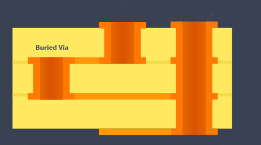
HDI stacked via structures are increasingly used in automotive electronics, industrial control systems, energy storage equipment, power converters, and advanced robotic control boards. By stacking laser-drilled microvias over buried vias, designers can achieve higher routing density and more efficient vertical interconnection in limited board space.
However, one manufacturing detail requires particular attention: how the buried via is prepared before the next HDI build-up layer is laminated.
When a laser microvia is designed to connect directly to a buried via, the buried via must provide a stable and reliable landing structure. In many stacked-via designs, this requires resin filling followed by copper plating or another qualified planarization process. An improperly prepared buried via can introduce risks involving interconnection, lamination quality, thermal reliability, insulation performance, and signal integrity.
This article explains what can happen when a buried via is not properly filled and planarized before HDI stacking and how to evaluate the manufacturing requirements during PCB design and supplier review.
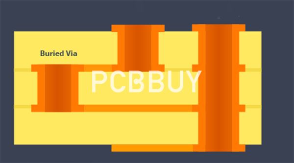
1. Electrical Interconnection: An Unfilled Buried Via Can Create an Unreliable Landing Point
The basic principle of a stacked-via structure is straightforward: a buried via completes an internal connection, and a laser-drilled microvia from the next build-up layer connects to the prepared copper surface above it.
For this connection to be reliable, the laser microvia needs a properly defined conductive landing area. If the buried via remains an open internal cavity, the laser drilling and subsequent metallization process may not create the intended continuous interconnection.
Potential consequences include:
• Open circuits.
• High or unstable contact resistance.
• Incomplete copper connection at the via interface.
• Latent interconnection defects that may become more apparent during thermal or mechanical stress.
This is one reason why electrical testing alone should not be considered the only verification method for complex HDI stacked structures. Depending on the product requirements, dimensional inspection, microsection analysis, and appropriate electrical testing methods may all be needed.
For high-reliability designs, PCBBUY's manufacturing review can help evaluate whether the proposed stacked-via structure has a suitable process route before production begins.
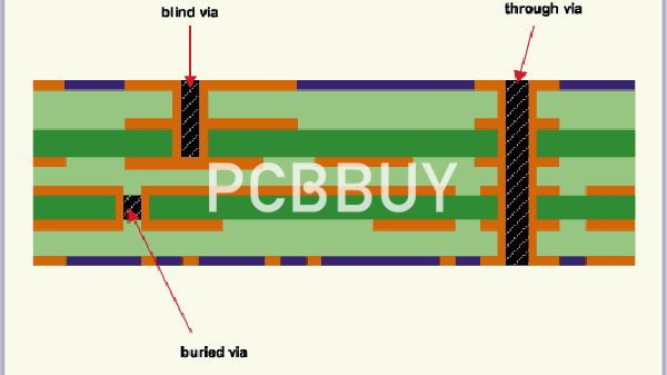
2. Lamination Quality: Internal Voids Can Affect Surface Planarity
An unfilled buried via is effectively an internal cavity. During subsequent lamination, prepreg resin flows under heat and pressure to bond the PCB layers together. The behavior of this resin depends on the stack-up, cavity geometry, resin flow characteristics, and lamination process.
If the via cavity is not properly managed, localized surface irregularities may develop above the buried via. In stacked-via applications, these irregularities can affect the geometry of the next laser-drilled microvia and make process control more difficult.
Possible concerns include:
• Localized depressions or uneven surfaces.
• Variations in dielectric thickness above the buried via.
• Increased difficulty in controlling laser drilling depth.
• Local copper geometry changes around the stacked-via area.
For high-density designs, surface planarity is especially important because microvias, fine-pitch pads, and BGA escape routing may all occupy a limited area.
The appropriate filling and planarization process should therefore be determined during the PCB engineering review rather than treated as a secondary production detail.
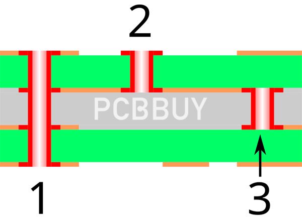
3. Thermal Reliability: Stacked Via Structures Must Withstand Repeated Stress
Automotive, industrial, power, and energy-storage electronics can experience repeated temperature changes during manufacturing and operation. A multilayer HDI PCB may also undergo several thermal processes, including lamination and component assembly.
Copper and PCB dielectric materials have different thermal expansion characteristics. In complex stacked-via structures, material interfaces and geometry changes can concentrate mechanical stress.
If an internal cavity or poorly controlled interface remains in the buried-via area, it may become a localized structural weakness. Under repeated thermal stress, potential reliability concerns can include:
• Cracking at copper-to-dielectric interfaces.
• Separation or degradation around the via structure.
• Changes in electrical continuity.
• Localized delamination in severe cases.
The actual reliability risk depends on the PCB material, stack-up, via dimensions, copper structure, assembly conditions, and operating environment. For this reason, high-reliability applications should define appropriate qualification and inspection requirements based on the intended product use.
For automotive electronics, industrial control, and power applications, PCBBUY can review the stack-up and manufacturing data to help identify process-sensitive structures before fabrication.
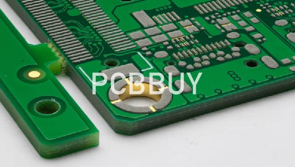
4. Long-Term Insulation Reliability and Moisture Exposure
Internal interfaces and material discontinuities can also affect long-term insulation performance, particularly in high-temperature and high-humidity environments.
Conductive anodic filament (CAF) formation and other electrochemical reliability concerns are influenced by several factors, including:
• PCB material properties.
• Moisture exposure.
• Electrical bias.
• Conductor spacing.
• Glass-resin interfaces.
• Manufacturing quality and material integrity.
An unfilled or poorly controlled internal via structure may create additional interfaces that need careful process control. In dense HDI designs, where conductor spacing can be limited, maintaining a consistent and well-bonded dielectric structure becomes even more important.
Resin filling and appropriate planarization can help create a more controlled structure for subsequent HDI processing. However, the filling material, curing process, and final construction should always be evaluated as part of the complete PCB reliability design.
5. Signal Integrity: Stacked Vias Need Predictable Geometry
One advantage of HDI technology is the ability to reduce unnecessary via stubs and create more efficient interconnections for high-density and high-speed designs.
However, signal integrity benefits depend on the physical consistency of the interconnection structure. An unexpected cavity, irregular copper geometry, or variation in dielectric thickness can introduce changes to the electrical characteristics of a high-speed signal path.
Potential effects may include:
• Local impedance discontinuities.
• Additional signal reflection.
• Changes in parasitic capacitance or inductance.
• Reduced signal margin in high-speed applications.
The severity depends on the signal frequency, rise time, via geometry, stack-up, and surrounding reference planes. Therefore, not every stacked via requires the same level of process control.
For demanding applications, impedance requirements and via structures should be reviewed together. PCBBUY can support engineering communication on multilayer and HDI PCB designs where stack-up and interconnection geometry require manufacturing evaluation.
Common Manufacturing Considerations for HDI Stacked Vias
|
Manufacturing consideration |
Why it matters |
|
Buried via filling |
Helps eliminate or control internal cavities before subsequent processing |
|
Surface planarization |
Provides a more consistent surface for the next build-up layer |
|
Laser microvia landing area |
Supports reliable connection to the underlying conductive structure |
|
Resin and material compatibility |
Affects bonding and thermal performance |
|
Copper plating control |
Helps maintain interconnection quality and via geometry |
|
Microsection inspection |
Allows internal via structures to be evaluated directly |
FAQ
1. Can prepreg resin alone fill a buried via during lamination?
In some PCB constructions, resin flow during lamination may partially fill internal openings. However, this should not automatically be considered a substitute for a controlled via-filling process when the buried via is used as a landing structure for a stacked laser microvia.
For stacked-via designs, the required surface condition, copper continuity, and via geometry should be confirmed during engineering review.
2. How can I verify the quality of a stacked buried-via structure?
A practical verification plan may include several steps:
• Clearly define the stacked-via and filling requirements in the fabrication documentation.
• Review the structure during DFM and engineering analysis.
• Use microsection analysis when internal structure verification is required.
• Check for voids, incomplete filling, irregular interfaces, and copper connection quality.
• Define appropriate electrical and reliability tests based on the product application.
The exact inspection requirements should match the product specification rather than relying on a single universal test method.
3. Does every buried via need resin filling?
Not necessarily. The manufacturing requirement depends on how the buried via is used in the PCB structure.
If a buried via serves as part of a stacked-via connection or must support subsequent build-up processing, filling and planarization may be necessary. A buried via used only for internal layer interconnection may have different requirements.
The best approach is to evaluate the via function, stack-up, reliability target, and manufacturing process together.
4. Does via filling significantly increase PCB manufacturing cost?
Controlled resin filling and planarization add manufacturing steps and can increase cost. However, for stacked-via structures that require a reliable landing surface, the process may be necessary to achieve the intended design.
During the quotation and DFM stage, engineers should identify stacked-via relationships early so the required process can be included in the manufacturing plan.
5. What information should I provide to a PCB manufacturer for an HDI stacked-via design?
To support an effective engineering review, provide:
• PCB stack-up information.
• Via structure and layer-to-layer connection requirements.
• Finished hole and microvia requirements.
• Material requirements.
• Impedance requirements, where applicable.
• Reliability or application-specific requirements.
For projects involving automotive electronics, industrial control, power systems, energy storage, and advanced robotics, providing this information early allows PCBBUY to evaluate the manufacturability of the HDI structure and recommend an appropriate production approach.
Conclusion
In an HDI stacked-via design, the condition of the buried via before the next build-up stage can directly affect manufacturing consistency and long-term reliability.
An unfilled buried via may create an uncontrolled internal cavity, making it more difficult to achieve a predictable laser-via connection and a consistent laminated structure. Depending on the design, this can introduce risks involving electrical interconnection, surface planarity, thermal reliability, insulation performance, and signal integrity.
For this reason, engineers should identify stacked-via relationships during the design stage and define the required filling and planarization process clearly in the fabrication documentation. Working with a PCB manufacturer such as PCBBUY during the DFM stage can help verify the process route before production and support a more reliable HDI PCB for automotive, industrial, power, energy-storage, and robotics applications.
Industry Category