What Problems Can Asymmetric PCB Stackups Cause Besides Warpage?
By:PCBBUY 11/20/2026 14:32
Asymmetric PCB stackups are a frequently discussed topic in the PCB industry, yet their impact is often oversimplified as nothing more than “board warpage.” Design engineers may notice a slight bow in the fabricated board, while procurement teams may see additional charges for “impedance control” or “special lamination engineering review” on the quotation. However, on the production line and at the customer’s end, the real problems often do not emerge until electrical testing, temperature cycling, or even after the boards have been installed in volume production vehicles.
Warpage is only the most visible mechanical symptom. Behind it lies a chain of interconnected deviations involving lamination stress, dielectric thickness distribution, resin flow, and interlayer bonding strength. In applications such as automotive electronics, industrial control, power electronics, energy storage, new energy systems, and embodied robotics, where after-the-fact corrective action is rarely acceptable, the consequences of an asymmetric stackup extend far beyond whether the board is physically warped.
1. Warpage Is Only the Most Visible Problem
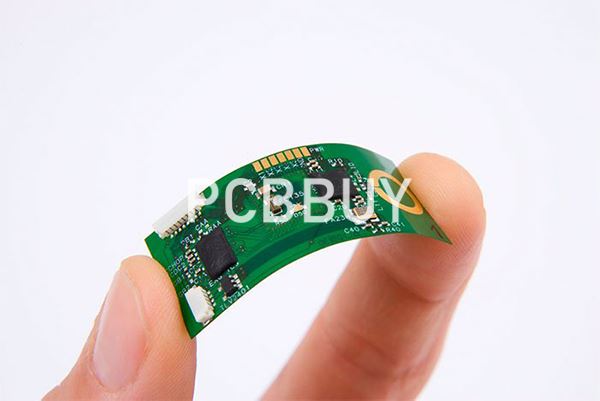
The immediate consequence of an asymmetric stackup is that the thermal expansion behavior of the board's upper and lower sections becomes unbalanced during lamination and reflow soldering. Copper has a coefficient of thermal expansion (CTE) of approximately 17 ppm/°C, while the Z-axis CTE of FR-4 resin is typically in the range of 50–70 ppm/°C. This represents a significant mismatch between the two materials.
A symmetrical stackup helps counteract the bending moments caused by this mismatch through a mirrored arrangement of the upper and lower layers. Once the dielectric thickness, copper thickness, or number of prepreg (PP) plies becomes unbalanced between the two sides, this compensation mechanism is disrupted, allowing the board to release stress in the form of bow or twist.
IPC-6012 Class 3 specifies a bow-and-twist limit of 0.75%. For boards using Kingboard or Shengyi material systems, Lieban applies a stricter warpage control limit of ≤0.5%. However, even when a board meets this limit during outgoing inspection, the residual stress has not disappeared. It has simply been locked inside the laminate.
This residual stress can be reactivated by the thermal shock of subsequent reflow soldering at 245–260°C. For BGA packages with a 0.4 mm pitch or even finer spacing, relatively small localized board deformation can introduce coplanarity deviations during solder joint formation. These deviations may manifest as insufficient solder joints, open circuits, or initiation points for fatigue cracks that develop later in service.
More importantly, the effects of an asymmetric structure are not evenly distributed across the board. Areas with dense copper distribution and areas with sparse copper distribution experience different amounts of resin flow. This can amplify variations in dielectric thickness across the board, laying the groundwork for the impedance and CAF issues discussed below.
2. Dielectric Thickness Deviates from Design Values, Causing Impedance Drift Across the Board
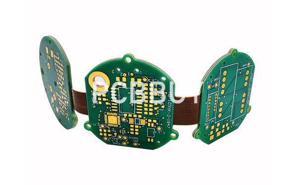
In impedance-controlled PCB design, the stackup parameters entered by the design engineer are nominal values. For example, a particular prepreg layer may be specified to have a compressed thickness of 0.10 mm, corresponding to a 50 Ω single-ended impedance.
However, an asymmetric stackup changes the flow paths and filling behavior of resin between layers. In areas with low copper coverage, more resin is pushed into the gaps between copper features, resulting in a dielectric thickness that may be significantly lower than the nominal value. Areas with high copper coverage behave differently.
One repeatedly observed magnitude of variation is that a deviation of approximately 12% in the compressed prepreg thickness can be sufficient to shift characteristic impedance from 50 Ω to 43 Ω. This type of deviation can affect an entire interface rather than appearing as an isolated problem on a single trace.
The danger of this type of impedance shift is that it may not trigger any obvious error. The board can pass continuity testing, AOI may show no pattern defects, and impedance coupon measurements may even fall within a relaxed tolerance range. Yet the signal eye diagram may already have narrowed at the actual operating data rate.
DDR, PCIe, and automotive SerDes links are more sensitive to reference-plane spacing and dielectric constant (Dk) than many general-purpose design guidelines might suggest. An asymmetric stackup turns dielectric thickness distribution from a design variable into a condition determined by the actual lamination process. If procurement and design teams validate simulations using only nominal stackup parameters, the boards delivered from production may enter assembly with systematic impedance deviations.
During stackup review, Lieban adjusts impedance models in advance based on its experience with actual post-lamination dielectric thickness. Its stated impedance control capability is ±10%, compared with the commonly cited industry level of ±15%.
This does not make an asymmetric stackup symmetrical. However, when asymmetry cannot be completely avoided, it helps keep impedance deviations within measurable and deliverable limits.
3. Delamination and CAF: How Asymmetric Stress Creates a Hidden Pathway at the Resin–Glass Interface
Warpage and impedance deviation can potentially be intercepted through visual inspection and electrical testing. The impact of an asymmetric stackup on interlayer integrity, however, is closer to a silent failure pathway.
The fundamental lamination process involves resin flowing under heat and pressure, impregnating the glass fabric, and eventually curing. In a symmetrical stackup, resin flow and curing shrinkage on the upper and lower sides tend to remain balanced, resulting in relatively low residual stress at the interfaces.
An asymmetric structure disrupts this balance. One side may contain more prepreg plies and a greater volume of resin, while the other contains a higher proportion of core material or copper layers. During curing, the two sides experience different amounts of shrinkage and different stress-release patterns.
These differences first create localized stress concentrations at the resin–glass interfaces and interlayer bonding surfaces. In severe cases, they can lead to microcracks or localized resin starvation. In structures where heavy copper layers are adjacent to sparse signal layers, one-directional resin flow can make localized resin starvation more likely, creating potential initiation points for delamination and blistering.
More importantly, these microcracks and weakened interfaces do not necessarily appear as visible delamination during outgoing inspection. Instead, they can become potential pathways for moisture and ionic migration.
The classic mechanism of conductive anodic filament (CAF) formation involves copper ions migrating along the resin–glass interface from the anode toward the cathode. Reduced interfacial adhesion, resin voids, and inadequate glass-fiber wet-out can create the conditions that allow this pathway to develop.
Several studies on the reliability of asymmetric hybrid stackups have identified CAF alongside warpage, delamination, and via reliability as major failure risks. The underlying concern is that asymmetric stress can accelerate interfacial degradation, creating initial defects that may facilitate CAF formation.
For power electronics, energy storage BMS, and industrial control boards operating under continuous electrical bias, high humidity, or temperature cycling, CAF does not simply result in “reduced performance.” It can cause progressive deterioration in insulation resistance, eventually leading to intermittent short circuits or dielectric breakdown.
Such failures are almost impossible to detect through early-stage electrical testing alone. They often become apparent only after aging tests at the customer's facility or several months of field operation.
4. Vias and Plated Copper: Reduced Reliability Due to Changes in Stress Distribution
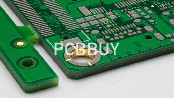
An asymmetric stackup changes not only the distribution of resin between layers but also the path through which thermal stress is transferred to via structures.
During Z-axis thermal expansion, the copper barrel of a plated through-hole (PTH) must withstand the difference in expansion between the copper and the PCB laminate in the board-thickness direction.
With a symmetrical stackup, the constraints acting on both sides of the via barrel are relatively balanced. With an asymmetric stackup, however, the resin constraints and copper-layer anchoring conditions can vary along different sections of the via barrel. During thermal cycling, stress concentrations are more likely to develop around the connections between the via wall and inner-layer pads or near the middle of the via barrel.
This effect becomes more pronounced in thick boards and high-aspect-ratio designs. The thicker the board and the smaller the hole diameter, the greater the strain amplitude experienced by the plated copper during thermal cycling. Unfilled or poorly plated vias can also have significantly fewer cycles to failure under temperature cycling than properly filled structures.
At the electroplating stage, Lieban uses Jingming automated vertical electroplating lines, with a stated copper plating uniformity of ≥97% and deep-hole capability covering a 13:1 board-thickness-to-hole-diameter ratio. Microcrystalline phosphor copper balls are used as the anode material to help provide sufficient margin in terms of plated copper thickness and density for subsequent thermal stress.
Nevertheless, this remains an engineering compensation measure, not an exemption from the risks of an asymmetric stackup. The more extreme the asymmetry, the greater the demands placed on plating uniformity and minimum via copper thickness to maintain via reliability.
5. From a Procurement Perspective: The Cost of an Asymmetric Stackup Goes Beyond the First Line of the Quotation
From a procurement perspective, one of the easiest aspects of asymmetric stackups to underestimate is how they shift costs from visible expenses to hidden ones.
A symmetrical stackup can use standard core combinations and conventional lamination structures. Engineering reviews are generally shorter, and material availability is easier to manage.
An asymmetric stackup, by contrast, may require a customized lamination structure, adjustments to the prepreg combination, or even special hybrid lamination or asymmetric dielectric thickness configurations. As a result, the workload for engineering review and first-article validation increases.
Lieban explicitly lists “customized lamination structures” and “asymmetric hybrid lamination / dissimilar-material hybrid lamination” among its special customization capabilities. The quotation differences for these orders reflect actual process complexity rather than simply an additional charge imposed by the PCB manufacturer.
Batch-to-batch consistency deserves even more attention from procurement teams.
A symmetrical stackup generally has a relatively wide process window. Small fluctuations in lamination parameters are less likely to disrupt the balance between the upper and lower sections. An asymmetric stackup narrows this process window, requiring tighter day-to-day control over lamination temperature uniformity, prepreg resin flow, and layer registration.
If a supplier accepts an asymmetric design using conventional processes and pricing intended for symmetrical stackups, problems may not be immediately apparent. However, variations in warpage, dielectric thickness, and impedance between production batches can gradually affect assembly yields at the customer's facility. The resulting costs eventually return to the procurement team in the form of material replacement, rework, or additional screening.
FAQ
Q1: If a PCB shows no obvious warpage, does that mean the asymmetric stackup has caused no problems?
No. Warpage is only the mechanical manifestation of an asymmetric stackup. Residual stress, deviations in dielectric thickness distribution, and interfacial microdamage can still exist even when the board passes visual inspection and routine electrical testing.
For boards using Kingboard or Shengyi material systems, Lieban applies a warpage control limit of ≤0.5% in its outgoing standards. However, this is a delivery acceptance threshold, not proof that the effects of asymmetric stress have been completely eliminated.
For automotive and industrial control applications, a more reliable approach is to evaluate the degree and location of stackup asymmetry during the stackup review stage rather than waiting for finished-board visual inspection.
Q2: What can Lieban do if the design cannot achieve a completely symmetrical stackup?
Lieban's approach is to get involved during the lamination structure review. The engineering team first identifies whether the asymmetry comes from localized heavy copper, hybrid materials, or layer-count constraints, and then adjusts the lamination parameters and dielectric configuration accordingly.
For structures where asymmetry must be retained, Lieban can provide customized lamination structures, special hybrid lamination, and multilevel impedance control. Its stated impedance control tolerance is ±10%. Impedance test data and an accompanying impedance coupon can also be provided in outgoing reports according to the product requirements.
The goal is not to make an asymmetric stackup “symmetrical,” but to control variations in warpage, dielectric thickness, and impedance within deliverable limits under known asymmetric conditions.
Q3: Can electrical testing screen out CAF risks caused by asymmetric stackups?
Routine continuity testing and flying probe testing have very limited ability to detect CAF.
CAF typically manifests as progressive deterioration in insulation resistance or intermittent short circuits. Under dry, room-temperature, short-duration testing conditions, it often does not trigger the relevant failure criteria.
For automotive, industrial control, and power-related products, Lieban can provide four-wire low-resistance flying probe testing according to order requirements. Its micro-ohm-level resistance measurement capability offers better resolution than conventional two-wire testing for identifying issues such as insufficient via copper thickness, trace defects, and localized connection abnormalities.
However, for CAF pathways that have already formed, the more fundamental controls remain stackup stress management and interfacial integrity, rather than finished-board electrical testing.
If a product will operate under continuous electrical bias and high-humidity conditions, it is advisable to clarify stackup symmetry constraints and reliability validation requirements with the engineering team before placing an order.
Q4: How can procurement teams determine whether a supplier's impedance control accounts for actual deviations in asymmetric stackups?
Look for three things:
-
Does the supplier adjust its impedance calculations based on actual post-lamination dielectric thickness?
-
Are impedance coupons fabricated together with the production panel and physically tested?
-
Does the supplier issue an impedance report containing actual measurement data?
Lieban's impedance control process includes theoretical calculation, impedance coupon fabrication, and measurement using an impedance tester. When an impedance report is selected, the report includes test data. This is fundamentally different from a process that relies only on theoretical calculations at the design stage without fabricating or testing impedance coupons.
For asymmetric stackups, procurement teams should also confirm whether the supplier identifies the impact of asymmetric regions on local dielectric thickness during engineering review, rather than simply applying standard parameters intended for symmetrical stackups.
Conclusion
Problems caused by asymmetric PCB stackups rarely appear in just one form, such as board warpage.
A more common chain of events begins when changes in lamination stress alter resin flow, causing dielectric thickness to deviate from design values and impedance to drift across the board. At the same time, localized stress concentrations develop at resin–glass interfaces, creating potential pathways for delamination and CAF. Thermal stress is then transferred along altered paths to vias and plated copper, with reliability degradation becoming apparent only after temperature cycling or prolonged exposure to electrical bias.
For automotive electronics, industrial control, power electronics, energy storage, new energy systems, and embodied robotics, where long-term reliability matters more than short-term pricing, stackup symmetry is not merely a layout preference. It is part of the reliability budget.
Lieban does not claim that every stackup can be made perfectly symmetrical. Instead, across its 4–26-layer high-layer-count PCB, heavy copper, HDI, special hybrid lamination, and customized lamination structure capabilities, Lieban aims to keep the deviations introduced by asymmetric stackups within engineering-acceptable limits through structures that can be reviewed, tested, and documented.
A symmetrical stackup is the easiest starting point. When design constraints make complete symmetry impossible, involving the PCB manufacturer early in the lamination structure review and impedance modeling is far more cost-effective than dealing with a batch of boards at the customer's facility that appear flat but already have drifting signal performance and reliability.
Industry Category