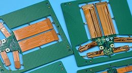
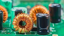
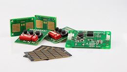
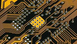
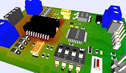
What Is Causing Supply Chain Disruptions in PCB Industry?
Populations worldwide are hard hit, and governments are struggling to establish and institute measures to slow the growth of COVID-19, which has claimed more than one and a half million lives thus far. In the US, the effects have been exceedingly high, with approximately 14 million cases of infection and 274,000 deaths as of December 3, 2020, according to the Centers for Disease Control (CDC). Additionally, the Bureau of Labor Statistics (BLS) found that roughly 50 million people were out of work due to the pandemic in May 2020.
PCB Instant Quote
.my-button {
display: inline-block;
padding: 10px 50px;
font-size: 16px;
text-align: center;
text-decoration: none;
background-color: blue;
color: #fffff0;
border: none;
border-radius: 5px;
font-weight: bold;
cursor: pointer;
box-shadow: 0px 2px 5px rgba(0, 0, 0, 0.3);
transition: background-color 0.3s ease, transform 0.3s ease;
}
.my-button:hover {
background-color: #C23C30;
transform: scale(1.05);
}
From an economic perspective, the pandemic has caused enormous instability. For example, the US economy showed a record of 33.1% annualized growth in Q3. However, this followed a record decline of 31.4% in the previous quarter, according to IPC’s November 2020 Economic Outlook report. In the PCB industry, imports are finally back up after steep initial declines—in Y/Y %—not seen since the recession of 2008-09. During that same period, PCB bookings across North America showed growth from the previous year. As many electronics OEMs and manufacturers rely on component imports, these types of interruptions can wreak havoc on end-use products’ delivery.
How to avoid supply chain disruptions in PCB industry?
With all of the problems with the global supply chain just discussed, OEMs need some practical ideas on how to avoid the disruptions that can derail their circuit board manufacturing. Here are some that should help.
Avoid using popular parts that are in short supply
On a new design, make sure to consult with your PCB manufacturing partner on the components list long before you commit to using those parts in the design. They will be able to advise you of which parts are available. It is also a good idea to use components with alternatives that can serve as form, fit, and functional replacements if need be. Another good idea is to leave room on the board for part changes that might not be exact form and fit replacements. Some of the parts you may be forced to use may only be available in older and larger package sizes or multiple component configurations.
Engage your manufacturing partner early
In addition to verifying the component availability in your design, the earlier your PCB contract manufacturer can start procuring the parts, the better. The extra amount of time will give them a chance to work with longer lead-time components or work alternative sources through their supply chain network. With more time up-front, the CMs engineering department will also have more opportunities to examine your design and recommend potential circuitry changes to avoid short-supply parts.
Be prepared to adjust your schedule and budget accordingly
If some of your parts do end up being in short supply, be prepared to make some changes. You may need to reset expectations with your marketing department and other key players and expand your schedule to accommodate longer lead times. You may also have to pay higher prices or allocate more funds for redesigns to work around some component shortages.
The key to avoiding supply chain disruptions in PCB assembly is to be ready for the unexpected, and the best place to start is by leaning on your manufacturer for help.
When it comes to supplying electronic products such as printed circuit boards, you need to prevent shortages. A deficit happens when the demand for a service or product exceeds the available supply. When such a situation occurs, you term the market to be in a disequilibrium state. On most occasions, this condition is temporary, with the products getting replenished and the market regaining equilibrium.
To avoid interruption to the electronics manufacturing supply chain, you’ll be in good hands dealing with firms that have strategies that deal with delays as a buyer. For printed circuit board distributors, they need to have in hand strategies to deal with shortages, such as collaborating with their suppliers, unlocking their ERP system, increasing accountability, ownership, and transparency among your clients.
Unexpected natural disasters may have some damaging effects on the electronics manufacturing supply chain. They bring about pauses when it comes to delivery. Generally, delays, interruptions due to weather, and inconsistency regarding supply and demand are common during such times.
For example, Hurricane Florence that hit the United States was the costliest storm around the world. It brought substantial damage to warehouses, disrupting roads and rail transport, and significantly impacted the U.S. economy by over 177 billion U.S Dollars.
While there is no practical way of predicting natural disasters, effective ways, and coping strategies such as developing disaster recovery and response plans provide detailed directions and guidelines for everybody responsible.
Additionally, maintaining excellent contact with external suppliers is essential. It ensures suppliers have robust procedures to analyze risk, avoid potential problems, and mitigate effects that may come with unforeseen outcomes. To avoid getting your electronics delivered late, you may have to deal with an electronics manufacturing firm with procedures for handling natural disasters that are either unforeseen or foreseen.
PCB Knowledge ⋅ 03/01/2022 10:36