Comprehensive Guide to the Benefits of Rigid-Flex PCBA
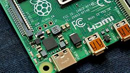
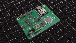
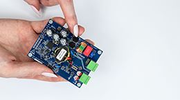
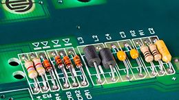
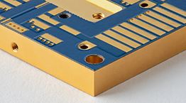
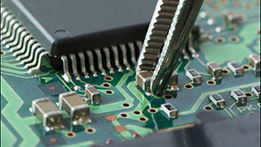
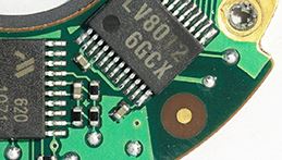
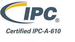
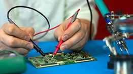
The flexibility of design and reliability of the design have emerged as two key innovation drivers in the rapidly changing electronics PCB industry. Rigid- Flex PCBA technology can be described as one of the most advanced printed circuit solutions in the contemporary world. This paper will discuss the advantages of rigid-flex PCBA, its operating principles and how PCBBUY has used global manufacturing skills to provide high-quality and reliable products to its customers around the world.PCB Instant Quote1. Understanding the Basics: What Is Rigid-Flex PCBA?A Rigid-Flex PCBA is the type of printed circuit board which is integrated into a rigid and flexible structure in one. The stiff parts ensure mechanical integrity and component support, and the flexible layers can be bent and folded, so the space-constrained 3D designs are possible that are not possible with rigid PCBs. Due to this special design, they do not require connections and cables separately therefore, making the assembly of assemblies lighter, thinner and more durable. We have mastered the art of producing rigid-flex assemblies of high-quality PCB IPC Class 3 and ISO9001 requirements at PCBBUY. The multilayer lamination, laser drilling and accurate alignment make sure that the layers bond perfectly even in high mechanical stress. 2. The Core Benefits of Rigid-Flex PCBANow, we can consider the main advantages of rigid-flex PCBA and why it is becoming more and more popular in such industries as automotive, medical devices, and consumer electronics. The design of the car is small, with space optimization. 2.1 Compact Design and Space Optimization Space saving is one of the major advantages that rigid-flex PCBA offers. Through rigidity and flexibility of sections designers will be able to do away with bulky connectors and cables, and shrink the size and weight of board. The rigid-flex assemblies are therefore best suited to the small and high-density devices like a smartphone, camera, and wearable electronics. In PCBBUY the engineers apply the latest tools of CAD layout optimization and impedance simulation to make sure that every square millimeter of the board is used productively without compromising on performance. 2.2 Increased Reliability and Durability.The conventional assemblies, which are supported by connectors and solder joints, are more prone to mechanical failure because of vibration and movement. Rigid-flex PCBAs, however, are less interconnected, i.e. less possible points of failure. This will lead to increased mechanical stability and increased product life span.PCBBUY conducts considerable bending and thermal cycle tests in order to prove the reliability of every rigid-flex board. All the products are AOI inspected, X-ray layer aligned and flying probe tested, to guarantee zero defects before delivery. 2.3 Improved Electricity Performance. The other key advantage of rigid-flex PCBA is that it has better electrical properties. The reduced interconnection routes result in less signal loss and less impedance variation which is essential to high-speed and high-frequency circuits. In PCBBUY, the steps in the fabrication process are controlled impedance design, microstrip and stripline optimization, and signal integrity analysis. This gives it a stable transmission even in multilayer structures. High frequency rigid-flex boards are commonly applied in radar systems, communication modules, and sophisticated sensors. 2.4 Design Flexibility and Assembly Efficiency. Rigid-flex assemblies ensure creative and compact mechanical designs can flex and fold in order to fit within tight enclosures. This suits them in the next-generation devices like folding smartphones, small medically powered devices and aerospace modules. PCBBUY provides Design-for-Flexibility (DFF) and Design-for-Manufacturability (DFM) services at the very beginning of your project. Our engineers also cooperate with customers to optimize the choice of materials, bending radius, and copper trace layout, which will ensure the performance or its manufacturability. 2.5 Long-Term Cost Efficiency Although the rigid-flex PCBA can be more expensive than a normal rigid board in the first fabrication, it saves costs in the long-term by providing better durability, less labor in assembly, and less in terms of maintaining the product. The total ownership cost (TOC) throughout the product lifecycle is minimized by minimizing the need to use more connectors and minimizing the possibility of having to rework.The integrated service of PCBBUY, i.e., BOM control, component sourcing, SMT assembly, and functional check also simplifies the process and allows customers to attain cost effectiveness and time savings. 3. PCBBUY’s Expertise in Rigid-Flex PCBA ManufacturingPCBBUY has been a trusted name in PCB and PCBA manufacturing for years, known for precision, consistency, and global service capability. Here’s how we ensure excellence in every rigid-flex PCBA we produce:3.1 Advanced Manufacturing TechnologyOur production lines feature high-precision laser drilling, automated optical inspection (AOI), controlled lamination systems, and vacuum-assisted pressing. We maintain stringent process control to guarantee alignment accuracy within ±25μm and impedance tolerance under ±10%.3.2 Strict Quality and Reliability StandardsAll PCBBUY rigid-flex PCBAs are built under IPC-A-600 Class 2/3 and ISO 13485 standards. Each board undergoes electrical testing, thermal aging validation, and mechanical stress analysis. These rigorous checks ensure consistent reliability across all production batches.3.3 End-to-End Support and Fast DeliveryFrom prototype fabrication to mass production, PCBBUY provides flexible lead times and global logistics support. Customers can track production progress in real-time through our online platform and receive detailed quality reports with every shipment. 4. Applications That Benefit from Rigid-Flex PCBAThe benefits of rigid-flex PCBA make it suitable for a wide range of industries:Consumer Electronics: Smartphones, cameras, wearablesAutomotive: ADAS systems, infotainment modules, sensorsMedical Devices: Portable diagnostic tools, implantsIndustrial Equipment: Robotics, automation control systemsAerospace: Navigation and communication systemsPCBBUY partners with clients from each of these sectors to develop optimized designs tailored for performance, miniaturization, and reliability. 5. Why Choose PCBBUY for Your Rigid-Flex PCBA ProjectsChoosing PCBBUY means more than just selecting a manufacturer—it’s choosing a long-term technical partner.Our customers value our transparent quotation system, strict process control, and high-yield production lines. Whether you’re developing a prototype or scaling up to full production, PCBBUY ensures that your rigid-flex PCBA meets the highest standards of quality and consistency.From prototype to production — PCBBUY delivers reliable rigid-flex PCBA with precision and trust. 6. ConclusionThe benefits of rigid-flex PCBA are clear: it combines the durability of rigid boards with the flexibility of flexible circuits, offering exceptional reliability and space efficiency. As electronics continue to evolve toward more compact and high-performance designs, rigid-flex technology will play an even greater role in the future.With PCBBUY’s advanced production capabilities and engineering expertise, you can bring your innovative designs to life faster and more reliably. Contact PCBBUY today to discuss your next rigid-flex PCBA project and experience world-class manufacturing firsthand. 7. FAQ: Common Questions About Rigid-Flex PCBAQ1: What makes rigid-flex PCBA more reliable than traditional PCB assemblies? A: Because rigid-flex assemblies reduce the number of connectors and solder joints, they eliminate common failure points. This results in improved durability and reliability under vibration, heat, and mechanical stress.Q2: Does PCBBUY support small-batch or prototype orders for rigid-flex PCBA? A: Absolutely. PCBBUY provides flexible production options, from one-off prototypes to high-volume manufacturing, with consistent quality across all batches.Q3: How does PCBBUY ensure consistent quality in rigid-flex PCBA production? A: Every PCBBUY board goes through automated optical inspection (AOI), X-ray verification, and electrical testing before shipment. We also follow strict IPC Class 3 standards for critical applications.
PCB Knowledge ⋅ 10/21/2025 16:05