Understanding SMT Assembly Capabilities
Surface Mount Technology (SMT) is at the core of modern electronic product manufacturing. From consumer electronics to industrial control systems and IoT applications, the quality of SMT assembly directly affects device performance, reliability, and lifespan. Therefore, when evaluating a manufacturing partner, understanding their SMT assembly capabilities becomes essential.
As a professional PCB fabrication and PCBA provider, PCBBUY has developed complete SMT production lines, strong engineering expertise, and stable supply chain support to handle both prototyping and mass production with consistent quality. This article explains what defines SMT assembly capabilities and how PCBBUY ensures high-precision, reliable, and efficient SMT assembly services.
PCB Instant Quote
.my-button {
display: inline-block;
padding: 10px 50px;
font-size: 16px;
text-align: center;
text-decoration: none;
background-color: blue;
color: #fffff0;
border: none;
border-radius: 5px;
font-weight: bold;
cursor: pointer;
box-shadow: 0px 2px 5px rgba(0, 0, 0, 0.3);
transition: background-color 0.3s ease, transform 0.3s ease;
}
.my-button:hover {
background-color: #C23C30;
transform: scale(1.05);
}
1. Introduction to SMT Assembly Capabilities
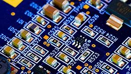
SMT assembly refers to mounting electronic components directly onto PCB surfaces without drilling through-hole leads. Its efficiency and precision make it the most widely used assembly method worldwide. However, not all SMT assembly lines deliver the same accuracy and reliability. The true strength of SMT assembly capabilities lies in:
Placement accuracy
Component size compatibility
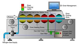
Reflow soldering stability
Automated inspection coverage
Process repeatability and manufacturing consistency
PCBBUY focuses on meeting high-mix, high-density assembly needs with optimized process control, ensuring stable quality from sample verification to large-scale production.
2. What Defines Professional SMT Assembly Capabilities?
Several key technical indicators define the maturity of SMT assembly capabilities:
Capability Factor
Explanation
Placement Accuracy
Determines how precisely components are aligned on the PCB pads.
Supported Component Sizes
Ability to assemble fine-pitch BGA, CSP, and micro-components such as 0402/0201/01005.
Reflow Soldering Profile Control
Ensures solder melting and wetting without damaging components.
Inspection and Testing Coverage
Includes AOI, X-ray, ICT, and FCT for solder joint reliability.
Mixed Assembly Support
Ability to combine SMT, THT, and wave soldering technologies in one board.
These indicators directly determine manufacturing yield, electrical stability, and long-term reliability of assembled boards.
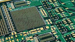
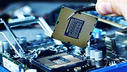
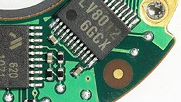
3. Core SMT Assembly Capabilities at PCBBUY
PCBBUY's SMT production lines are equipped with advanced pick-and-place machines, precision stencil printers, intelligent reflow ovens, and full-camera AOI/X-ray inspection systems. The core capabilities include:
PCBBUY SMT Capability
Technical Details
High-Speed Pick & Place Machines
Support for 01005 micro SMDs, BGA, QFN, CSP packages; ±0.025mm placement tolerance.
Automated Solder Paste Printing
Laser-cut stainless-steel stencils + SPI inspection for optimized solder volume.
Advanced Reflow Soldering Profiles
Lead-free and leaded reflow profiles, multi-zone temperature control.
Comprehensive Optical & X-ray Inspection
Ensures correct solder joints, especially for hidden pads (BGA / QFN).
Mixed Technology Assembly
SMT + THT + selective wave soldering, suitable for complex PCBA.
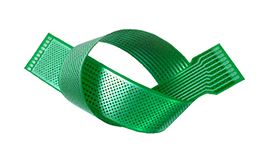
These capabilities allow PCBBUY to handle high-density layouts, multi-layer PCBs, flexible-rigid boards, and miniaturized components with high stability.
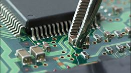
4. SMT Assembly Workflow at PCBBUY
A structured workflow ensures high-quality results in every batch:
PCB Incoming Quality Inspection
Stencil & Solder Paste Printing
SPI (Solder Paste Inspection)
High-Speed Pick-and-Place Assembly
Reflow Soldering Profile Optimization
AOI Inspection for Solder Quality
X-Ray Verification for BGA/QFN
Functional or Electrical Testing (FCT/ICT)
Final Visual Inspection & Packaging
Each stage is monitored according to IPC-A-610 standards to maintain repeatability and yield stability.
5. Component Sourcing and BOM Engineering Support
PCBBUY supports multiple sourcing models:
Customer-supplied BOM components
Turnkey component procurement (Digikey, Mouser, Arrow, etc.)
Cost-reduction and alternative sourcing suggestions
Traceable anti-counterfeit supply chain management
Our engineering team provides DFM (Design for Manufacturability) reviews to identify risks early and optimize assembly reliability before production starts.
6. Quality Assurance Standards at PCBBUY
PCBBUY adheres to strict manufacturing quality frameworks:
IPC-A-610 Class 2 / Class 3 compliance
ISO9001 quality management system
Full ESD protection during handling and storage
Moisture-sensitive device (MSD) humidity-controlled baking and sealing
Thermal cycle testing, vibration testing, and reliability evaluation (optional)
7. Industries Benefiting from PCBBUY SMT Assembly Capabilities
Our SMT assembly services support:
Consumer electronics and smart devices
Medical device circuit boards
Industrial sensors and automation control units
Automotive electronics and advanced driver systems
Aerospace & high-reliability boards
PCBBUY’s flexibility makes it suitable for both prototyping and large-scale batch production.
8. Why Choose PCBBUY for SMT Assembly?
One-stop fabrication + component procurement + assembly service
Fast lead time and stable delivery control
Strong engineering support throughout the product lifecycle
Competitive cost structure with transparent process management
PCBBUY is committed to delivering reliable, repeatable, and high-performance SMT manufacturing to support your product success.
9. FAQ About SMT Assembly Capabilities
Q1: What is the smallest component size PCBBUY can assemble? We support component sizes down to 01005 and fine-pitch BGA/CSP.
Q2: Can PCBBUY provide turnkey assembly services? Yes. We offer full PCB fabrication, component sourcing, and SMT assembly service.
Q3: Do you provide DFM (Design for Manufacturability) review? Yes, our engineers review PCB stackup, pad designs, spacing, and BOM risks before production.
Q4: What inspection methods are used in SMT assembly? AOI, SPI, X-Ray, ICT, FCT, and manual QC for comprehensive quality control.
PCB Knowledge ⋅ 10/31/2025 17:41