How to prevent PCB warpage?
During the manufacturing of PCB, the boards are easy to be bended or warped. How to prevent the issues? In this passage, we will talk about the topic and please follow us and read the content below for more information.
PCB Instant Quote
.my-button {
display: inline-block;
padding: 10px 50px;
font-size: 16px;
text-align: center;
text-decoration: none;
background-color: blue;
color: #fffff0;
border: none;
border-radius: 5px;
font-weight: bold;
cursor: pointer;
box-shadow: 0px 2px 5px rgba(0, 0, 0, 0.3);
transition: background-color 0.3s ease, transform 0.3s ease;
}
.my-button:hover {
background-color: #C23C30;
transform: scale(1.05);
}
What are the causes of PCB warpage?
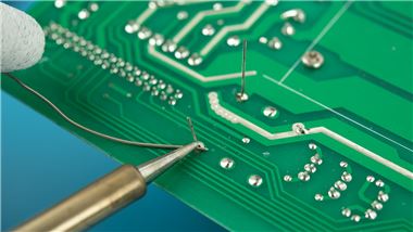
SMT is also known as surface mount technology. In the manufacturing process, solder paste is heated and melted under a kind of heating environment, so that PCB solder pad can be reliably combined with surface mount components by solder paste alloy. We call this process reflow soldering. When the circuit board passes Reflow (Reflow soldering), it is easy for the plate to bend and become warped. In serious cases, it may even lead to empty soldering and erecting of components.
In the automatic insert line, if the printing plate is not smooth, it will cause inaccurate positioning, and the components cannot be inserted into the hole and surface of the plate, and even break the automatic insert machine. The welded plates with the components are bent, and the component feet are difficult to be cut in order. The boards can’t fit into the case or the socket, so it’s equally annoying for an assembly plant to get stuck on the board. At present, the PCB has entered the era of surface mounting and chip mounting, and the assembly plant must be more and stricter.
According to IPC – 6012, specification for the identification and performance of rigid PCB, the maximum permissible warp and twist for surface mounting of PCB is 0.75%, and other boards allow 1.5%. This is an improvement over IPC – RB – 276. Currently, the warping degree approved by each electronic assembly plant, whether double-sided or multilayer, is 1.6mm thick, usually 0.70~0.75%, and many SMT, BGA boards require 0.5%. Some electronics factories are agitating to increase the standard of warpage to 0.3% and test the warpage using gb4677.5-84 or ipc-tm-650.2.4.22b. Put the printing plate on the platform to be checked, and insert the test pin into the place with the maximum warp.
The reason for the formation of each plate bending and plate warping may be different, but it should be attributed to the stress applied on the plate is greater than the stress that can be borne by the plate material. The following are the four causes of plate bending and plate warping.
1. The area of the copper surface on the circuit board is not uniform, which will deteriorate the bending and warping of the board
General circuit boards will be designed with a large area of copper foil for grounding, sometimes Vcc layer design has a large area of copper foil, when these large areas of copper foil can not evenly distributed in the same circuit boards, will cause uneven heat and cooling speed, circuit boards, of course, also can heat bilges cold shrink, if increases and cannot at the same time can cause different stress and deformation, the temperature of the board at this time if the Tg has reached the upper limit value, the board will start to soften, causing permanent deformation.
2. The weight of the board itself will cause the sag deformation of the board
Generally, the backweld furnace will use the chain to drive the circuit board forward in the backweld furnace, that is, the whole board will be supported by the fulcrum on both sides of the board.
3. The depth and connection of v-cut will affect the deformation of the panel
Basically, v-cut is the culprit of damaging the structure of the board, because v-cut is to Cut the v-groove on the original large sheet of board, so the place where v-cut is prone to deformation.
4. The connection points (vias) of each layer on the circuit board will limit the expansion and contraction of the board
Nowadays, the board is mostly multi-layered, and there will be rivet-like connection points (via) between the layers. The connection points are divided into through-hole, blind hole and buried hole. Where there are connection points, the effect of expansion and contraction of the board will be limited, and also the bending and warping of the board will be indirectly caused.
How to prevent PCB warpage?
how can we better prevent the PCB from warping in the manufacturing process? Here are a few effective methods to help you.
1. Effect of reducing temperature on stress of plates
Since “temperature” is the main source of plate stress, so as long as the temperature of the backweld furnace is reduced or the rate of temperature rise and cooling of the slow plate in the backweld furnace is adjusted, the situation of plate bending and plate warping can be greatly reduced. There may be other side effects, such as solder shorts.
2. High Tg plate
Tg is the glass transition temperature, which is the temperature at which the material changes from glass state to rubber state. The lower the Tg value of the material, the faster the board begins to become soft after entering the back welding furnace, and the longer the time to become soft rubber state, the more serious the deformation of the board will of course be. The use of a sheet with a higher Tg can increase its ability to withstand stress and deformation, but the relative cost of the material is also higher.
Increase the thickness of the circuit board
Many electronic products in order to achieve the purpose of the thinner, the thickness of the board has the 1.0 mm and 0.8 mm, and even do the thickness of 0.6 mm, the thickness of this to keep the board with no deformation after welding furnace back, really stand, suggested that if there is no frivolous request, the board is best can use 1.6 mm thickness, can greatly reduce the risk of plate bending and deformation.
4. Reduce the size of circuit boards and the number of panels
Since most of the back weld furnace use chain to drive circuit board, the larger the size of the circuit board will be because of the weight of its own, concave deformation in the welding furnace back, so try to put the long side of the circuit board as an edge on the chain back to soldering furnace, can reduce weight sag deformation caused by the circuit board itself, to reduce the number of the makeup is also for this reason, that is to say, a furnace, as far as possible with narrow edge perpendicular to the direction of the furnace, can achieve the lowest sag deformation.
5. Used tray jig
If the above methods are difficult to achieve, the last is to use a stove tray (reflow carrier/template), to reduce the deformation of a furnace tray can reduce the plate bending plate become warped because both thermal and cold, all hope that the tray can hold the circuit board to wait until the temperature of the circuit board below the Tg values began to harden, can also maintain the original size.
If the single-layer tray is not able to reduce the deformation of the circuit board, it is necessary to add a cover, the circuit board with the upper and lower two tray clamping, so that the problem of the circuit board back welding furnace deformation can be greatly reduced. However, this furnace tray is expensive, but also has to add artificial storage and recovery tray.
6. Switch to Router instead of v-cut’s divider
Since the v-cut will destroy the structural strength of the boards, try not to use the v-cut divider or reduce the depth of the v-cut.
7. Three penetration points in engineering design:
A. The arrangement of semi-solidified sheets between layers should be symmetrical, for example, six layers, the thickness between 1~2 and 5~6 layers should be the same as the number of sheets of the semi-cured sheets, otherwise the lamination will be prone to warp.
B. Multi-layer core board and semi-cured sheet shall use the same supplier’s product.
C. The graphic area of the circuit on the outer surface A and B should be as close as possible. If face A is A large copper surface, while face B only walks A few lines, this kind of printing plate is easy to warp after etching. If the two sides of the line area difference is too large, the thin side can be added some independent grid to balance.
8. Longitude and latitude of semi-cured tablets:
The warp and weft shrinkage rates of semi-cured sheet after lamination are different. Otherwise, after the lamination is easy to cause the finished plate warping, even if the pressure drying plate is difficult to correct. Many of the reasons for the warping of multilayer plates are due to the fact that the laminates on the laminates are not clearly separated from the latitude and longitude of the semi-cured sheets.
The method of differentiating the longitude and latitude directions: the rolled semi-solidified sheet is rolled in the longitude direction and the width direction in the latitude direction. For copper foil, the long edge is zonal and the short edge is meridional. If not sure, you can contact the manufacturer or supplier.
9. Straightening of thin plate plating:
Special clamping rolls should be made when 0.4~0.6mm ultra-thin multilayer plates are used for plate surface plating and pattern plating. After the thin plates are clamped on the fly bar of automatic plating line, a round rod is used to string up the clamping rolls on the whole fly bar, so as to straighten all the plates on the roller, so that the plates after plating will not be deformed. If this measure is not taken, after electroplating the copper layer of 20 or 30 microns, the thin plate will be bent and difficult to remedy.
10. Cooling of board after hot air leveling:
The hot air of the printed board is impacted by the high temperature of the solder groove (about 250 degrees Celsius) at ordinary times. After taking out, it should be put on the flat marble or steel plate for natural cooling and then sent to the post-processing machine for cleaning. This is good for warping the board. In some factories, to enhance the brightness of the surface of the lead tin, the hot air of the board is immediately put into cold water after leveling, and a few seconds later is taken out for post-processing. In addition, air float bed can be added to the equipment for cooling.
PCB Knowledge ⋅ 07/22/2021 16:40