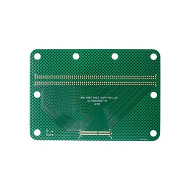
PCB components
PCBs are very important in the whole PCB manufacturing process.But how to choose the best manufacturing board components? A lot are standardized off-the-shelf parts that you can fast identify, find, and purchase. You’ll achieve your PCB assembly process faster if you know the parts that you need. Printed circuit boards are essential in the manufacturing process of a circuit board. But how do you go about choosing the best manufacturing board components?
PCB Instant Quote
.my-button {
display: inline-block;
padding: 10px 50px;
font-size: 16px;
text-align: center;
text-decoration: none;
background-color: blue;
color: #fffff0;
border: none;
border-radius: 5px;
font-weight: bold;
cursor: pointer;
box-shadow: 0px 2px 5px rgba(0, 0, 0, 0.3);
transition: background-color 0.3s ease, transform 0.3s ease;
}
.my-button:hover {
background-color: #C23C30;
transform: scale(1.05);
}
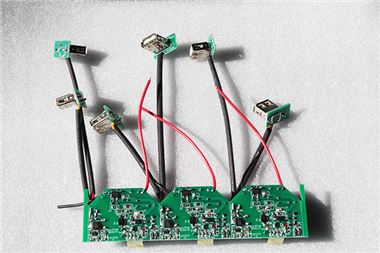
While Electronic components process information in form of electrical signals, a Printed Circuit Board PCB is the skeletal structure on which the electronic components are mounted and soldered to hold them together and provide pathways for information to flow between components through PCB traces.
Some of the most commonly used electronic components are resistors, capacitors, inductors, diodes, LEDs, transistors, crystals and oscillators, electromechanical components like relays and switches, ICs, and connectors. These components have terminals and are available in specific standardized packages that the designer can choose to suit his application. SMT (Surface Mount Technology) and Through-hole are the two types of mounting techniques used to place components on a PCB.
What are the types of PCB components?
What is Resistor?
Resistors are one of the most commonly used components in PCBs and is a passive electrical component whose function is to introduce resistance to the flow of electric current in an electrical circuit to limit the current. Their function is to resist the flow of current by dissipating electric power as heat. They come in a multitude of different types made of a range of different materials but the classic resistor most familiar to the hobbyist is the ‘axial’ style resistors with leads on both long ends and the body inscribed with colored rings. These rings are a code that indicates their resistance value.
What is Capacitor?
The Capacitor is a passive electrical component, whose function is to store electrical energy and deliver it to the circuit when needed. The function of capacitors is to temporarily hold electric charge, and release it whenever more power is needed elsewhere in the circuit. Typically, it does this by collecting opposite charges on two conductive layers separated by an insulating, or dielectric, material. Capacitors are often categorized according to the conductor or dielectric material, which gives rise to many types with varying characteristics from high capacitance electrolytic capacitors, diverse polymer capacitors to the more stable ceramic disc capacitors. Capacitors fall into two categories: Polarized and non-polarized.
What is Inductor?
The Inductors is a passive two-terminal electrical component that stores magnetic energy when an electric current is passed through it. It’s an insulated wire wound into a coil around a core of some material (air, iron, powdered iron, or ferrite material) in a spiral form. The simplest inductor is a coil of wire. The greater the number of windings, the greater the magnetic field and therefore inductance. This serves to amplify the magnetic field substantially and therefore, the stored energy. Inductors are often used to filter out or block certain signals, for example, blocking interference in radio equipment or used in conjunction with capacitors to manipulate AC signals in switched mode power supplies.
What is Potentiometer?
Potentiometers are a form of variable resistor. They are commonly available in rotary and linear types. By rotating the knob of a rotary potentiometer, resistance is varied as the slider contact is moved over a semi-circular resistor. The linear potentiometer is the same, except that resistance is varied by moving the slider contact on the resistor linearly.
What is Transistor?
Several billions may be found in a single IC chip. But transistors are simply amplifiers and electronic switches. They come in several types, with the bipolar transistor as the most common type. They can be further categorized into NPN and PNP versions. Bipolar transistors have 3 pins – the base, collector and emitter. For an NPN type, when a small current flows through from the base to the emitter, then it turns on another circuit that causes lager current to flow from the collector to the emitter. In a PNP transistor, the directions are reversed.
What is Diode?
The diode is two terminal semiconductor devices that allow an electric current to pass in one direction. It allows current to flow in one direction only, from the anode (+) to the cathode (-). It does this by having zero resistance in one direction and high resistance via the other direction. This feature can be used to block current from flowing in the wrong direction, which could cause damage. Typical material used in a diode is silicon and germanium. They conduct when a minimum forward voltage is applied across it and remain off during reverse bias condition.
What is SCR?
SCR is short for Silicon Controlled Rectifiers, also known as thyristors, are similar to transistors and diodes. Actually, they are essentially two transistors working together. They also have three leads but consist of four silicon layers instead of three and only function as switches, not amplifiers. Another important difference is that only a single pulse is required to activate the switch, whereas current has to be applied continuously in the case of a single transistor. They are more suited to switching larger amounts of power.
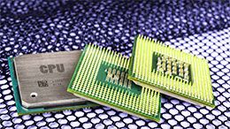
What is IC?
ICs, known as integrated circuits are exactly that, they are circuits and components that have been shrunk down onto wafers of semiconductor material. The sheer number of components that can be fit onto a single chip is what gave rise to the first calculators and now powerful computers from smart phones to supercomputers. They are usually the brains of a wider circuit. The circuit is typically encased in a black plastic housing which can come in all shapes and sizes and have visible contacts.
What is Crystal Oscillator?
Crystal oscillators provide the clock in many circuits that require precise and stable timing elements. They produce a periodic electronic signal by physically causing a piezoelectric material, the crystal, to oscillate, hence the name. Each crystal oscillator is designed to vibrate at a specific frequency and more stable, economical and have a small form factor compared to other timing methods.
What is Switch and Relay?
The switch is simply a power button to control the current flow in the circuit, by switching between an open or a closed circuit. Similarly, a relay is an electromagnetic switch operated via a solenoid, which becomes like a sort of temporary magnet when current flows through it. They function as switches and can also amplify small currents to larger currents.
What is Sensor?
Sensors are devices and the function is to detect changes in environmental conditions and generate an electrical signal corresponding to that change, which is sent to other electronic components in the circuit. Sensors convert energy from a physical phenomenon into electrical energy, and so they are in effect, transducers. They can be anything from a type of resistor in a resistance temperature detector (RTD), to LEDs detecting in-fared signals, such as in a television remote.
PCB Glossary ⋅ 05/06/2021 17:58