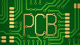
Flying Probe Testing in PCB Manufacturing:
Introduction to Flying Probe Testing in PCB Manufacturing
Flying probe testing in PCB manufacturing has become an essential quality assurance process in today’s electronics industry. Unlike traditional in-circuit testing (ICT), which requires expensive and time-consuming test fixtures, flying probe testing relies on flexible and highly precise moving probes to verify the electrical performance of printed circuit boards.
At PCBBUY, we leverage advanced flying probe testing equipment to guarantee high reliability, accuracy, and speed in prototype verification and small-to-medium batch PCB production. This capability reflects our strong commitment to quality and innovation in PCB manufacturing.
PCB Instant Quote
.my-button {
display: inline-block;
padding: 10px 50px;
font-size: 16px;
text-align: center;
text-decoration: none;
background-color: blue;
color: #fffff0;
border: none;
border-radius: 5px;
font-weight: bold;
cursor: pointer;
box-shadow: 0px 2px 5px rgba(0, 0, 0, 0.3);
transition: background-color 0.3s ease, transform 0.3s ease;
}
.my-button:hover {
background-color: #C23C30;
transform: scale(1.05);
}
What is Flying Probe Testing in PCB Production?
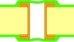
Flying probe testing is a method that uses multiple high-speed probes that move along the X and Y axes to make direct contact with pads, vias, and test points on a PCB. By applying electrical signals and measuring responses, it checks for open circuits, short circuits, impedance issues, and faulty components.
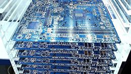
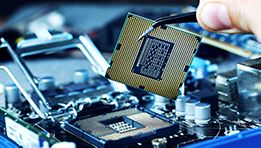
Unlike ICT, flying probe testing does not require a custom test fixture, which significantly reduces cost and lead time. This makes it ideal for prototype runs, engineering validation, and boards with complex, high-density designs such as HDI PCBs and multi-layer PCBs.
Advantages of Flying Probe Testing for PCB Manufacturing
Choosing flying probe testing provides numerous advantages:
No Fixture Cost – Reduces the need for costly fixtures, saving both time and money.
Fast Turnaround – Ideal for prototype and small-batch verification where time-to-market is critical.
High Precision – Accurately detects open circuits, shorts, and subtle electrical parameter deviations.
Flexible Application – Suitable for BGA, HDI, and 4–32 layer PCBs.
Cost Efficiency – More economical than ICT, especially for frequent design changes.
At PCBBUY, these advantages translate into greater efficiency, faster prototyping cycles, and reliable quality for our global customers.
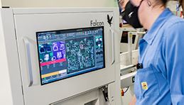
Flying Probe Testing Process at PCBBUY
At PCBBUY, our flying probe testing process is designed for accuracy, speed, and traceability. The steps include:
Test Program Preparation – We generate testing programs directly from customer-provided Gerber files or netlist data.
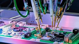
Automated Probe Movement – High-precision probes move rapidly across test points, contacting vias, pads, and solder joints.
Electrical Testing – The system performs multiple tests, including:
Open/short circuit detection
Resistance, capacitance, and inductance measurement
Diode/Transistor polarity checks
Impedance matching verification
Data Output & Reporting – A detailed electronic report is generated, showing test results, detected issues, and pass/fail analysis.
This process ensures defect-free delivery and provides customers with full traceability, which is especially important for high-reliability industries such as aerospace, medical devices, and telecommunications.
Applications of Flying Probe Testing in PCB Manufacturing
Flying probe testing is widely applied in different production stages and industries:
Prototype Validation – Ensures design functionality before mass production.
Small-Batch Production – Ideal for projects requiring flexibility and frequent design updates.
High-Reliability Sectors – Used in medical electronics, automotive, aerospace, and 5G communications.
Complex PCB Designs – Perfect for HDI, multi-layer, and fine-pitch BGA assemblies.
At PCBBUY, we optimize flying probe testing for each application scenario to meet customer-specific needs.
PCBBUY’s Capabilities in Flying Probe Testing
PCBBUY has invested in state-of-the-art flying probe testers that support a wide range of PCB types and complexity levels. Our core capabilities include:
Support for 4–32 layer PCBs with fine pitch components.
Advanced high-speed probing systems that achieve accurate measurements within microns.
Rapid test programming from Gerber/netlist files, minimizing preparation time.
Comprehensive test coverage for electrical continuity, component verification, and functional analysis.
International quality compliance – Strictly adhering to IPC-9252 standards and ISO-certified processes.
By integrating these advanced capabilities, PCBBUY ensures that every board shipped meets the highest standards of performance and reliability.
Why Choose PCBBUY for Flying Probe Testing
There are many PCB manufacturers offering flying probe testing, but PCBBUY stands out due to:
Technical Expertise – Our engineering team has extensive experience in advanced PCB testing and design validation.
Cost-Effective Solutions – Eliminate fixture costs while maintaining maximum accuracy.
Full Traceability – Detailed test reports for each board enhance customer confidence.
Flexible Service Models – From prototypes to small and medium batch runs.
Global Customer Support – Trusted by international clients for consistent quality and fast delivery.
Partnering with PCBBUY means you gain a reliable, professional, and efficient PCB manufacturing partner.
Conclusion
Flying probe testing in PCB manufacturing is no longer optional—it is a critical process to ensure performance, reliability, and long-term durability. At PCBBUY, we combine advanced flying probe testing equipment with years of manufacturing expertise to deliver top-quality PCBs that meet international standards.
If you are looking for a trusted partner for prototype PCB production, small-batch manufacturing, or high-reliability boards, PCBBUY’s flying probe testing solutions will ensure your products are built to perform.
👉 Contact PCBBUY today to learn more about our flying probe testing services and request a customized PCB manufacturing solution.
FAQ: Flying Probe Testing in PCB
Q1: When should I use flying probe testing instead of ICT? Flying probe testing is best for prototypes, small batches, or boards with frequent design changes since it eliminates fixture costs and reduces lead time.
Q2: What is the maximum PCB layer count supported by PCBBUY’s flying probe testing? PCBBUY supports flying probe testing for PCBs ranging from 4 layers up to 32 layers, including HDI designs.
Q3: How accurate is flying probe testing at PCBBUY? Our advanced equipment achieves micrometer-level accuracy in electrical measurements, ensuring defect-free results.
Q4: Does PCBBUY provide detailed flying probe test reports? Yes. Each PCB tested at PCBBUY comes with a comprehensive report that includes test coverage, measurement data, and defect analysis for full traceability.
PCB Knowledge ⋅ 08/19/2025 16:06