PCB Copper Clad Laminate for Material Fundamentals and Manufacturing Considerations
Introduction
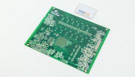
PCB copper clad laminate is the foundation of all printed circuit boards. Its material properties directly affect PCB reliability, electrical performance, and manufacturing stability.
For this reason, understanding pcb copper clad laminate is essential not only for designers, but also for manufacturers responsible for process control. As PCB designs become more complex, proper laminate selection and processing play a critical role in achieving consistent quality.
PCB Instant Quote
.my-button {
display: inline-block;
padding: 10px 50px;
font-size: 16px;
text-align: center;
text-decoration: none;
background-color: blue;
color: #fffff0;
border: none;
border-radius: 5px;
font-weight: bold;
cursor: pointer;
box-shadow: 0px 2px 5px rgba(0, 0, 0, 0.3);
transition: background-color 0.3s ease, transform 0.3s ease;
}
.my-button:hover {
background-color: #C23C30;
transform: scale(1.05);
}
What Is PCB Copper Clad Laminate?
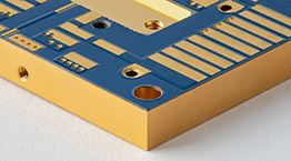
PCB copper clad laminate (CCL) is a composite material consisting of a dielectric substrate bonded with one or more layers of copper foil. It serves as the base material from which PCB circuits are formed through imaging, etching, drilling, and lamination processes. The quality and consistency of the copper clad laminate determine how well these processes perform during fabrication.
Common Types of PCB Copper Clad Laminate
Standard FR-4 Copper Clad Laminate
FR-4 is the most widely used PCB copper clad laminate due to its balanced electrical, mechanical, and cost performance. It is suitable for a wide range of general-purpose electronic applications.
High-Tg Copper Clad Laminate
High-Tg laminates offer improved thermal stability compared to standard FR-4. They are commonly used in multilayer PCBs and lead-free assembly processes where higher operating temperatures are expected.
High-Frequency and Low-Loss Laminates
For high-speed and RF applications, low-loss copper clad laminates are used to minimize signal attenuation. These materials require more precise process control during fabrication.
Special-Purpose Copper Clad Laminates
Special laminates are designed for specific applications, such as high thermal conductivity or halogen-free requirements. Each type introduces unique processing considerations.
Key Properties of PCB Copper Clad Laminate
Dielectric Constant and Signal Performance
The dielectric constant of the laminate affects signal propagation speed and impedance control. Stable dielectric properties are essential for high-speed PCB designs.
Glass Transition Temperature (Tg)
Tg defines the temperature at which the laminate transitions from a rigid to a softer state. Higher Tg improves dimensional stability during lamination and assembly.
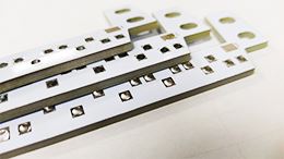
Copper Foil Type and Adhesion
Copper foil type and adhesion strength affect etching accuracy and long-term reliability. Strong copper-to-laminate bonding reduces the risk of delamination.
Thickness and Dimensional Stability
Uniform laminate thickness ensures accurate layer registration and consistent impedance across the PCB.
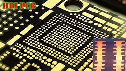
How Copper Clad Laminate Affects PCB Manufacturing?
PCB copper clad laminate influences multiple fabrication steps, including:
Lamination pressure and temperature behavior
Drilling quality and hole wall integrity
Etching performance and line definition
Dimensional stability during multilayer buildup
Stable laminate behavior simplifies process control and improves yield.
Manufacturing Challenges Related to Copper Clad Laminate
Different laminate types require different process adjustments. Common challenges include:
Resin flow control during lamination
Layer-to-layer alignment in multilayer boards
Drill wear and hole quality consistency
Handling and storage of sensitive materials
Managing these challenges requires both experience and process discipline.
How Manufacturing Capability Ensures Reliable Laminate Processing?
Material Qualification and Supplier Control
Consistent laminate performance starts with qualified material sources. Incoming material inspection ensures conformity before production begins.
Process Parameter Optimization
Lamination cycles, pressure profiles, and thermal control are optimized for each laminate type. This prevents defects such as delamination or warpage.
Inspection and Process Monitoring
In-process checks help ensure laminate-related variables remain within control limits throughout fabrication.
PCBBUY’s Experience with PCB Copper Clad Laminate
PCBBUY has extensive experience processing various pcb copper clad laminate types, including standard FR-4, high-Tg, and special application materials.
Through engineering-driven process control, PCBBUY supports stable production for both prototype and volume PCB orders.
Key strengths include:
Controlled lamination and drilling processes
Experience with multilayer and export-grade PCBs
Engineering support for material selection and DFM review
Consistent quality across different production volumes
This approach helps customers achieve reliable PCB performance without unnecessary manufacturing risk.
Design Considerations When Selecting Copper Clad Laminate
To achieve optimal results, designers should:
Match laminate properties to application requirements
Consider thermal and electrical performance together
Communicate material specifications clearly in fabrication notes
Engage manufacturers early for process compatibility review
Early collaboration helps reduce material-related production issues.
Conclusion
PCB copper clad laminate forms the structural and electrical foundation of every PCB. While material selection is important, manufacturing capability ultimately determines how well laminate properties are realized in the final product.
By combining material expertise with controlled manufacturing processes, PCBBUY helps customers achieve reliable PCB production based on pcb copper clad laminate performance.
FAQ
What is PCB copper clad laminate?
PCB copper clad laminate is the base material used in PCB fabrication. It consists of a dielectric substrate bonded with one or more layers of copper foil and forms the foundation for circuit pattern creation.
How does copper clad laminate affect PCB manufacturing?
Copper clad laminate directly influences lamination behavior, drilling quality, etching accuracy, and dimensional stability. Stable laminate performance helps improve yield and long-term PCB reliability.
What types of PCB copper clad laminate are commonly used?
Common types include standard FR-4, high-Tg laminates, high-frequency low-loss materials, and special-purpose laminates designed for thermal or environmental requirements.
Why is high-Tg copper clad laminate used in PCB manufacturing?
High-Tg laminates offer better thermal stability, making them suitable for multilayer PCBs and lead-free assembly processes where higher temperatures are involved.
How does copper foil quality impact PCB performance?
Copper foil quality affects trace adhesion, etching precision, and resistance to delamination. Strong copper-to-laminate bonding improves electrical and mechanical reliability.
What manufacturing challenges are related to copper clad laminate?
Challenges include resin flow control during lamination, layer registration in multilayer boards, drilling consistency, and handling of sensitive laminate materials.
How does PCBBUY ensure stable processing of copper clad laminate?
PCBBUY uses qualified laminate suppliers, controlled lamination parameters, and in-process inspection to ensure consistent copper clad laminate performance throughout PCB production.
Can PCBBUY support special PCB copper clad laminate materials?
Yes. PCBBUY supports a range of copper clad laminate types, including high-Tg and special-purpose materials, with engineering support for material selection and process compatibility.
What should designers consider when selecting PCB copper clad laminate?
Designers should consider electrical performance, thermal requirements, manufacturability, and cost balance, and communicate material specifications clearly during the design stage.
PCB Knowledge ⋅ 12/30/2025 15:36