6 Layer PCB vs 8 Layer PCB Manufacturing Differences to Capability Comparison
Introduction
As electronic products continue to increase in complexity, multilayer PCBs have become the standard solution for high-density and high-performance designs.
Among them, 6 layer PCB and 8 layer PCB are two commonly used configurations. Understanding the differences between 6 layer PCB vs 8 layer PCB is essential not only from a design perspective, but also from a manufacturing capability standpoint.
PCB Instant Quote
.my-button {
display: inline-block;
padding: 10px 50px;
font-size: 16px;
text-align: center;
text-decoration: none;
background-color: blue;
color: #fffff0;
border: none;
border-radius: 5px;
font-weight: bold;
cursor: pointer;
box-shadow: 0px 2px 5px rgba(0, 0, 0, 0.3);
transition: background-color 0.3s ease, transform 0.3s ease;
}
.my-button:hover {
background-color: #C23C30;
transform: scale(1.05);
}
What Is 6 Layer PCB?
A 6 layer PCB typically consists of multiple signal layers combined with dedicated power and ground planes. This structure provides improved routing flexibility and better signal integrity compared to simpler multilayer designs.
6 layer PCBs are commonly used in industrial electronics, consumer devices, and mid-speed digital applications.
What Is 8 Layer PCB?
An 8 layer PCB adds additional signal or plane layers, allowing for higher routing density and more controlled electrical performance. This configuration is often required for high-speed, high-frequency, or high-reliability electronic systems.
The increased layer count also introduces higher manufacturing complexity and stricter process control requirements.
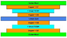
Stackup Structure Comparison
The difference between 6 and 8 layer PCBs becomes clear when examining their stackup options.
Feature
6 Layer PCB
8 Layer PCB
Typical Stackup
Signal + Power/Ground planes
Additional signal or plane layers
Routing Density
Moderate
High
Power Integrity
Good
Excellent
EMI Control
Limited improvement
Strong improvement
Design Flexibility
Balanced
Advanced
Manufacturing Process Differences
From a manufacturing perspective, moving from 6 to 8 layers significantly increases process complexity.
8 layer PCBs require:
More inner layer imaging steps
Tighter layer-to-layer registration control
Increased lamination pressure and temperature stability
Each additional layer amplifies the impact of small process variations.
Lamination and Registration Challenges
Lamination is one of the most critical steps in multilayer PCB manufacturing. For 8 layer PCBs, resin flow, prepreg selection, and lamination cycles must be precisely controlled.
Compared to 6 layer PCBs, 8 layer designs have stricter requirements for:
Layer alignment accuracy
Void prevention during lamination
Dimensional stability after thermal processing
Drilling and Via Reliability Considerations
Higher layer counts increase drilling depth and aspect ratio. This places higher demands on drilling accuracy and plated through-hole reliability.
8 layer PCBs often require tighter control over:
Drill bit wear
Hole wall quality
Copper plating uniformity
These factors directly affect long-term electrical reliability.
Electrical Performance and Signal Integrity
An 8 layer PCB provides greater flexibility in separating signal, power, and ground planes. This improves impedance control, reduces crosstalk, and enhances return path continuity.
While 6 layer PCBs can support many applications, 8 layer PCBs offer superior electrical performance for high-speed and high-density designs.
Manufacturing Yield and Quality Control
As layer count increases, manufacturing yield becomes more sensitive to process deviations. Effective quality control is essential to maintain consistent production results.
Aspect
6 Layer PCB
8 Layer PCB
Manufacturing Yield
Relatively stable
More sensitive to variation
Inspection Difficulty
Moderate
High
Electrical Testing
Standard
Enhanced focus required
Process Control Level
High
Very High
Cost vs Manufacturing Capability
Although 8 layer PCBs involve higher manufacturing cost, they also reflect stronger process capability. Manufacturers capable of producing stable 8 layer PCBs typically possess advanced lamination, drilling, and inspection systems. Choosing the right layer count should balance performance needs, reliability, and manufacturability.
PCBBUY’s Capability in 6 and 8 Layer PCB Manufacturing
PCBBUY has experience manufacturing both 6 layer and 8 layer PCBs for global customers. Through controlled lamination processes, precise registration management, and strict quality control, PCBBUY supports reliable multilayer PCB production.
Key capability strengths include:
Multilayer lamination expertise
Registration and drilling accuracy control
Export-oriented quality standards
Engineering support for stackup optimization
When to Choose 6 Layer PCB or 8 Layer PCB?
Designers should consider upgrading from 6 to 8 layers when:
Routing density exceeds practical limits
Signal integrity becomes critical
Power and ground plane isolation is required
EMI control needs improvement
Early consultation with the PCB manufacturer helps avoid unnecessary redesigns.
Conclusion
The comparison between 6 layer PCB vs 8 layer PCB highlights not only design differences, but also manufacturing capability requirements. While 6 layer PCBs remain suitable for many applications, 8 layer PCBs provide enhanced electrical performance and routing flexibility at the cost of increased manufacturing complexity.
Selecting an experienced manufacturer ensures that higher-layer PCBs deliver the expected performance and reliability.
FAQ
What is the main difference between a 6 layer PCB and an 8 layer PCB?
The main difference is the number of signal and plane layers, which affects routing density, power integrity, and manufacturing complexity.
Is an 8 layer PCB more difficult to manufacture than a 6 layer PCB?
Yes. An 8 layer PCB requires tighter lamination, registration, drilling, and quality control compared to a 6 layer PCB.
When should an 8 layer PCB be used instead of a 6 layer PCB?
An 8 layer PCB is recommended for high-speed, high-density, or EMI-sensitive applications where additional layers improve performance.
Does layer count affect PCB reliability?
Higher layer counts increase manufacturing complexity, but with proper process control, reliable 8 layer PCBs can be achieved.
Can PCBBUY manufacture both 6 layer and 8 layer PCBs?
Yes. PCBBUY supports both 6 layer and 8 layer PCB manufacturing with engineering-driven process control.
PCB Knowledge ⋅ 01/09/2026 14:40